ZHCSCV9A August 2014 – October 2014 ADS1120-Q1
PRODUCTION DATA.
- 1 特性
- 2 应用
- 3 说明
- 4 修订历史记录
- 5 Pin Configurations and Functions
- 6 Specifications
- 7 Parameter Measurement Information
-
8 Detailed Description
- 8.1 Overview
- 8.2 Functional Block Diagram
- 8.3
Feature Description
- 8.3.1 Multiplexer
- 8.3.2 Low-Noise PGA
- 8.3.3 Modulator
- 8.3.4 Digital Filter
- 8.3.5 Output Data Rate
- 8.3.6 Voltage Reference
- 8.3.7 Clock Source
- 8.3.8 Excitation Current Sources
- 8.3.9 Low-Side Power Switch
- 8.3.10 Sensor Detection
- 8.3.11 System Monitor
- 8.3.12 Offset Calibration
- 8.3.13 Power Supplies
- 8.3.14 Temperature Sensor
- 8.4 Device Functional Modes
- 8.5 Programming
- 8.6 Register Map
- 9 Application and Implementation
- 10Power-Supply Recommendations
- 11Layout
- 12器件和文档支持
- 13机械封装和可订购信息
5 Pin Configurations and Functions
PW Package
TSSOP-16
(Top View)
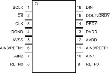
Pin Functions
| PIN | TYPE | DESCRIPTION | |
|---|---|---|---|
| NUMBER | NAME | ||
| 1 | SCLK | Digital input | Serial clock input |
| 2 | CS | Digital input | Chip select, active low. Connect to DGND if not used. |
| 3 | CLK | Digital input | External clock source pin. Connect to DGND if not used. |
| 4 | DGND | Digital | Digital ground |
| 5 | AVSS | Analog | Negative analog power supply |
| 6 | AIN3/REFN1 | Analog input | Analog input 3, negative reference input 1. Internal low-side power switch connected between AIN3/REFN1 and AVSS. Leave unconnected or tie to AVDD if not used. |
| 7 | AIN2 | Analog input | Analog input 2. Leave unconnected or tie to AVDD if not used. |
| 8 | REFN0 | Analog input | Negative reference input 0. Leave unconnected or tie to AVDD if not used. |
| 9 | REFP0 | Analog input | Positive reference input 0. Leave unconnected or tie to AVDD if not used. |
| 10 | AIN1 | Analog input | Analog input 1. Leave unconnected or tie to AVDD if not used. |
| 11 | AIN0/REFP1 | Analog input | Analog input 0, positive reference input 1. Leave unconnected or tie to AVDD if not used. |
| 12 | AVDD | Analog | Positive analog power supply |
| 13 | DVDD | Digital | Positive digital power supply |
| 14 | DRDY | Digital output | Data ready, active low. Leave unconnected or tie to DVDD using a weak pull-up resistor if not used. |
| 15 | DOUT/DRDY | Digital output | Serial data output combined with data ready, active low |
| 16 | DIN | Digital input | Serial data input |