ZHCSCV9A August   2014  – October 2014 ADS1120-Q1

PRODUCTION DATA.  

  1. 特性
  2. 应用
  3. 说明
  4. 修订历史记录
  5. Pin Configurations and Functions
  6. Specifications
    1. 6.1 Absolute Maximum Ratings
    2. 6.2 Handling Ratings
    3. 6.3 Recommended Operating Conditions
    4. 6.4 Thermal Information
    5. 6.5 Electrical Characteristics
    6. 6.6 SPI Timing Requirements
    7. 6.7 SPI Switching Characteristics
    8. 6.8 Typical Characteristics
  7. Parameter Measurement Information
    1. 7.1 Noise Performance
  8. Detailed Description
    1. 8.1 Overview
    2. 8.2 Functional Block Diagram
    3. 8.3 Feature Description
      1. 8.3.1  Multiplexer
      2. 8.3.2  Low-Noise PGA
        1. 8.3.2.1 PGA Common-Mode Voltage Requirements
        2. 8.3.2.2 Bypassing the PGA
      3. 8.3.3  Modulator
      4. 8.3.4  Digital Filter
      5. 8.3.5  Output Data Rate
      6. 8.3.6  Voltage Reference
      7. 8.3.7  Clock Source
      8. 8.3.8  Excitation Current Sources
      9. 8.3.9  Low-Side Power Switch
      10. 8.3.10 Sensor Detection
      11. 8.3.11 System Monitor
      12. 8.3.12 Offset Calibration
      13. 8.3.13 Power Supplies
      14. 8.3.14 Temperature Sensor
        1. 8.3.14.1 Converting from Temperature to Digital Codes
          1. 8.3.14.1.1 For Positive Temperatures (for Example, 50°C):
          2. 8.3.14.1.2 For Negative Temperatures (for Example, -25°C):
        2. 8.3.14.2 Converting from Digital Codes to Temperature
    4. 8.4 Device Functional Modes
      1. 8.4.1 Power-Up and Reset
      2. 8.4.2 Conversion Modes
        1. 8.4.2.1 Single-Shot Mode
        2. 8.4.2.2 Continuous Conversion Mode
      3. 8.4.3 Operating Modes
        1. 8.4.3.1 Normal Mode
        2. 8.4.3.2 Duty-Cycle Mode
        3. 8.4.3.3 Turbo Mode
        4. 8.4.3.4 Power-Down Mode
    5. 8.5 Programming
      1. 8.5.1 Serial Interface
        1. 8.5.1.1 Chip Select (CS)
        2. 8.5.1.2 Serial Clock (SCLK)
        3. 8.5.1.3 Data Ready (DRDY)
        4. 8.5.1.4 Data Input (DIN)
        5. 8.5.1.5 Data Output and Data Ready (DOUT/DRDY)
        6. 8.5.1.6 SPI Timeout
      2. 8.5.2 Data Format
      3. 8.5.3 Commands
        1. 8.5.3.1 RESET (0000 011x)
        2. 8.5.3.2 START/SYNC (0000 100x)
        3. 8.5.3.3 POWERDOWN (0000 001x)
        4. 8.5.3.4 RDATA (0001 xxxx)
        5. 8.5.3.5 RREG (0010 rrnn)
        6. 8.5.3.6 WREG (0100 rrnn)
      4. 8.5.4 Reading Data
      5. 8.5.5 Sending Commands
      6. 8.5.6 Interfacing with Multiple Devices
    6. 8.6 Register Map
      1. 8.6.1 Configuration Registers
        1. 8.6.1.1 Configuration Register 0 (offset = 00h) [reset = 00h]
        2. 8.6.1.2 Configuration Register 1 (offset = 01h) [reset = 00h]
        3. 8.6.1.3 Configuration Register 2 (offset = 02h) [reset = 00h]
        4. 8.6.1.4 Configuration Register 3 (offset = 03h) [reset = 00h]
  9. Application and Implementation
    1. 9.1 Application Information
      1. 9.1.1 Serial Interface Connections
      2. 9.1.2 Analog Input Filtering
      3. 9.1.3 External Reference and Ratiometric Measurements
      4. 9.1.4 Establishing a Proper Common-Mode Input Voltage
      5. 9.1.5 Pseudo Code Example
    2. 9.2 Typical Application
      1. 9.2.1 K-Type Thermocouple Measurement (-200°C to +1250°C)
        1. 9.2.1.1 Design Requirements
        2. 9.2.1.2 Detailed Design Procedure
        3. 9.2.1.3 Application Curves
      2. 9.2.2 3-Wire RTD Measurement (-200°C to +850°C)
        1. 9.2.2.1 Design Requirements
        2. 9.2.2.2 Detailed Design Procedure
          1. 9.2.2.2.1 Design Variations for 2-Wire and 4-Wire RTD Measurements
        3. 9.2.2.3 Application Curves
      3. 9.2.3 Bridge Measurement
        1. 9.2.3.1 Design Requirements
        2. 9.2.3.2 Detailed Design Procedure
  10. 10Power-Supply Recommendations
    1. 10.1 Power-Supply Sequencing
    2. 10.2 Power-Supply Decoupling
  11. 11Layout
    1. 11.1 Layout Guidelines
    2. 11.2 Layout Example
  12. 12器件和文档支持
    1. 12.1 文档支持
      1. 12.1.1 相关文档 
    2. 12.2 商标
    3. 12.3 静电放电警告
    4. 12.4 术语表
  13. 13机械封装和可订购信息

封装选项

机械数据 (封装 | 引脚)
散热焊盘机械数据 (封装 | 引脚)
订购信息

10 Power-Supply Recommendations

The device requires two power supplies: analog (AVDD, AVSS) and digital (DVDD, DGND). The analog power supply can be bipolar (for example, AVDD = 2.5 V, AVSS = –2.5 V) or unipolar (for example, AVDD = 3.3 V, AVSS = 0 V) and is independent of the digital power supply. The digital supply sets the digital I/O levels.

10.1 Power-Supply Sequencing

The power supplies can be sequenced in any order but in no case must any analog or digital inputs exceed the respective analog or digital power-supply voltage limits. Wait approximately 50 µs after all power supplies are stabilized before communicating with the device to allow the power-up reset process to complete.

10.2 Power-Supply Decoupling

Good power-supply decoupling is important to achieve optimum performance. AVDD, AVSS (when using a bipolar supply) and DVDD must be decoupled with at least a 0.1-µF capacitor, as shown in Figure 83 and Figure 84. Place the bypass capacitors as close to the power-supply pins of the device as possible using low-impedance connections. TI recommends using multi-layer ceramic chip capacitors (MLCCs) that offer low equivalent series resistance (ESR) and inductance (ESL) characteristics for power-supply decoupling purposes. For very sensitive systems, or for systems in harsh noise environments, avoiding the use of vias for connecting the capacitors to the device pins may offer superior noise immunity. The use of multiple vias in parallel lowers the overall inductance and is beneficial for connections to ground planes. TI recommends connecting analog and digital ground together as close to the device as possible.

ai_unipolar_supply_bas683.gif
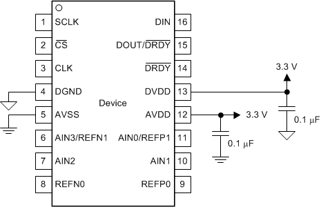
Figure 83. Unipolar Analog Power Supply
ai_bipolar_supply_bas683.gif
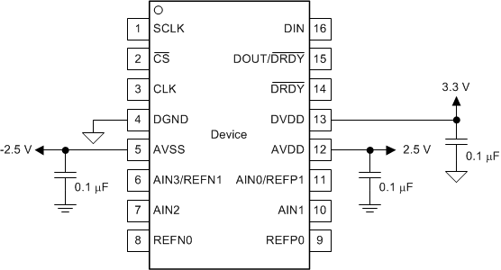
Figure 84. Bipolar Analog Power Supply