ZHCSHA5E july 2010 – july 2023 ADS1013-Q1 , ADS1014-Q1 , ADS1015-Q1
PRODUCTION DATA
- 1
- 1 特性
- 2 应用
- 3 说明
- 4 Revision History
- Device Comparison Table
- 5 Pin Configuration and Functions
- 6 Specifications
-
7 Detailed Description
- 7.1 Overview
- 7.2 Functional Block Diagrams
- 7.3
Feature Description
- 7.3.1 Multiplexer
- 7.3.2 Analog Inputs
- 7.3.3 Full-Scale Range (FSR) and LSB Size
- 7.3.4 Voltage Reference
- 7.3.5 Oscillator
- 7.3.6 Output Data Rate and Conversion Time
- 7.3.7 Digital Comparator (ADS1014-Q1 and ADS1015-Q1 Only)
- 7.3.8 Conversion Ready Pin (ADS1014-Q1 and ADS1015-Q1 Only)
- 7.3.9 SMbus Alert Response
- 7.4 Device Functional Modes
- 7.5 Programming
- 7.6 Register Map
-
8 Application and Implementation
- 8.1 Application Information
- 8.2
Typical Application
- 8.2.1 Design Requirements
- 8.2.2
Detailed Design Procedure
- 8.2.2.1 Shunt Resistor Considerations
- 8.2.2.2 Operational Amplifier Considerations
- 8.2.2.3 ADC Input Common-Mode Considerations
- 8.2.2.4 Resistor (R1, R2, R3, R4) Considerations
- 8.2.2.5 Noise and Input Impedance Considerations
- 8.2.2.6 First-Order RC Filter Considerations
- 8.2.2.7 Circuit Implementation
- 8.2.2.8 Results Summary
- 8.2.3 Application Curves
- 8.3 Power Supply Recommendations
- 8.4 Layout
- 9 Device and Documentation Support
- 10Mechanical, Packaging, and Orderable Information
7.5.3 Writing To and Reading From the Registers
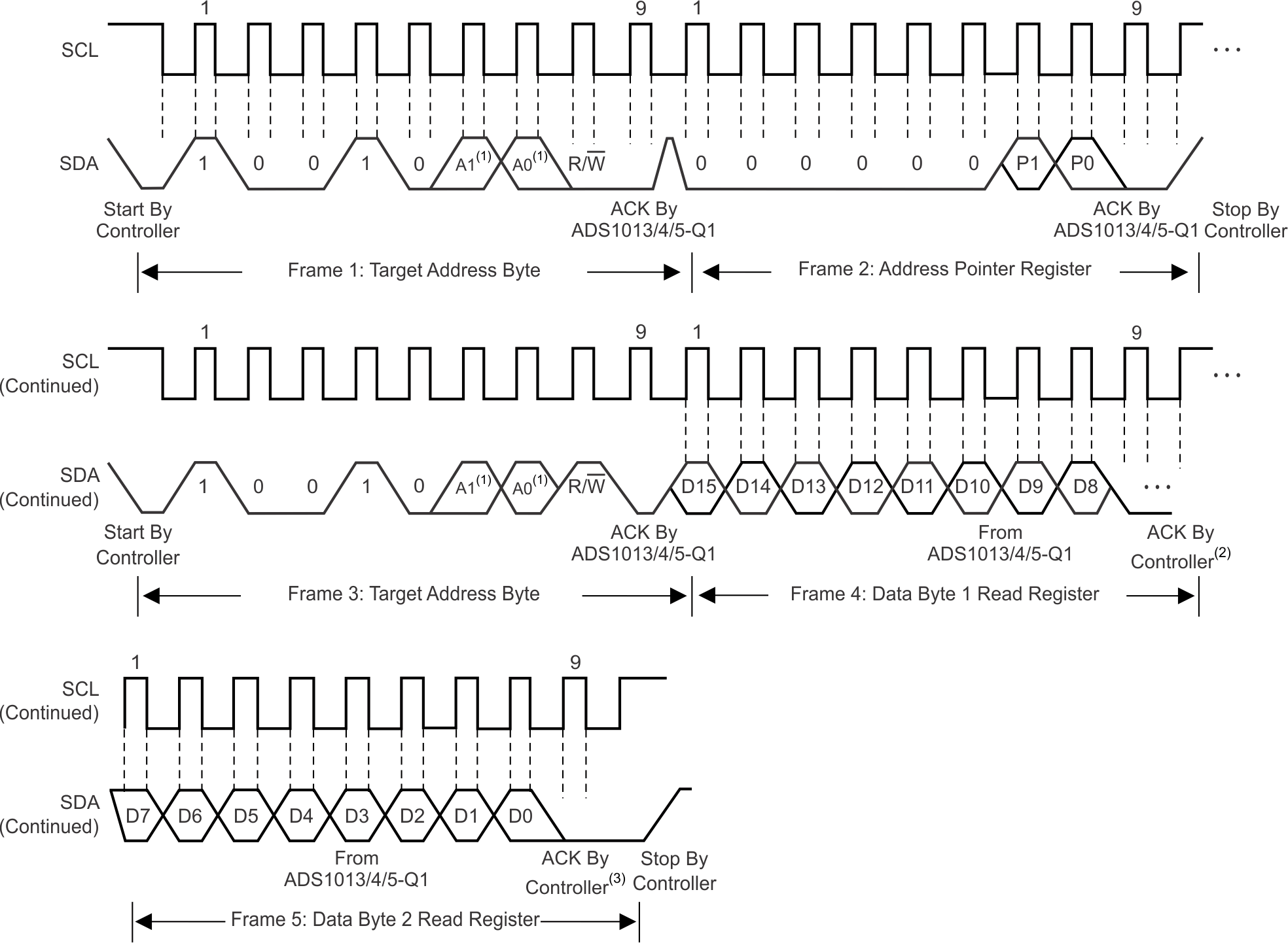
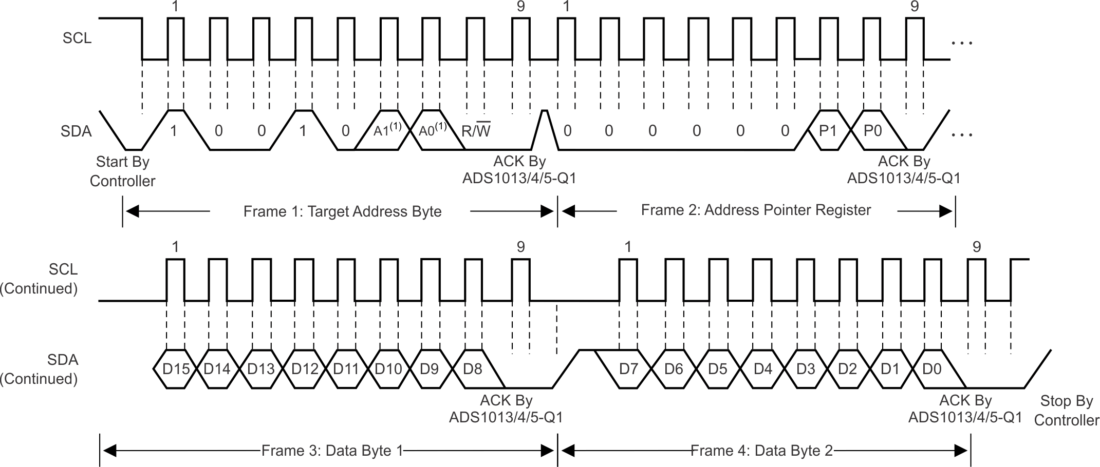
To access a specific register from the ADS101x-Q1, the controller must first write an appropriate value to register address pointer bits P[1:0] in the Address Pointer register. The Address Pointer register is written to directly after the target address byte, low R/W bit, and a successful target acknowledgment. After the Address Pointer register is written, the target acknowledges, and the controller issues a STOP or a repeated START condition.
When reading from the ADS101x-Q1, the previous value written to bits P[1:0] determines the register that is read. To change which register is read, a new value must be written to P[1:0]. To write a new value to P[1:0], the controller issues a target address byte with the R/W bit low, followed by the Address Pointer register byte. No additional data has to be transmitted, and a STOP condition can be issued by the controller. The controller can now issue a START condition and send the target address byte with the R/W bit high to begin the read. Figure 7-9 details this sequence. If repeated reads from the same register are desired, there is no need to continually send the Address Pointer register, because the ADS101x-Q1 store the value of P[1:0] until modified by a write operation. However, for every write operation, the Address Pointer register must be written with the appropriate values.


