ZHCSNC3B February   2021  – October 2022 ADC3561 , ADC3562 , ADC3563

PRODUCTION DATA  

  1. 特性
  2. 应用
  3. 说明
  4. Revision History
  5. Pin Configuration and Functions
  6. Specifications
    1. 6.1  绝对最大额定值
    2. 6.2  ESD 等级
    3. 6.3  建议运行条件
    4. 6.4  热性能信息
    5. 6.5  电气特性 - 功耗
    6. 6.6  电气特征 - 直流规格
    7. 6.7  电气特征 - 交流规格
    8. 6.8  时序要求
    9. 6.9  Typical Characteristics - ADC3561
    10. 6.10 Typical Characteristics - ADC3562
    11. 6.11 Typical Characteristics - ADC3563
  7. Parameter Measurement Information
  8. Detailed Description
    1. 8.1 Overview
    2. 8.2 Functional Block Diagram
    3. 8.3 Feature Description
      1. 8.3.1 Analog Input
        1. 8.3.1.1 Analog Input Bandwidth
        2. 8.3.1.2 Analog Front End Design
          1. 8.3.1.2.1 Sampling Glitch Filter Design
          2. 8.3.1.2.2 Analog Input Termination and DC Bias
            1. 8.3.1.2.2.1 AC-Coupling
            2. 8.3.1.2.2.2 DC-Coupling
        3. 8.3.1.3 Auto-Zero Feature
      2. 8.3.2 Clock Input
        1. 8.3.2.1 Single Ended vs Differential Clock Input
        2. 8.3.2.2 Signal Acquisition Time Adjust
      3. 8.3.3 Voltage Reference
        1. 8.3.3.1 Internal voltage reference
        2. 8.3.3.2 External voltage reference (VREF)
        3. 8.3.3.3 External voltage reference with internal buffer (REFBUF)
      4. 8.3.4 Digital Down Converter
        1. 8.3.4.1 DDC MUX for Dual Band Decimation
        2. 8.3.4.2 Digital Filter Operation
        3. 8.3.4.3 FS/4 Mixing with Real Output
        4. 8.3.4.4 Numerically Controlled Oscillator (NCO) and Digital Mixer
        5. 8.3.4.5 Decimation Filter
        6. 8.3.4.6 SYNC
        7. 8.3.4.7 Output Formatting with Decimation
      5. 8.3.5 Digital Interface
        1. 8.3.5.1 Output Formatter
        2. 8.3.5.2 Output Bit Mapper
        3. 8.3.5.3 Output Scrambler
        4. 8.3.5.4 Output Interface/Mode Configuration
          1. 8.3.5.4.1 Configuration Example
        5. 8.3.5.5 Output Data Format
      6. 8.3.6 Test Pattern
    4. 8.4 Device Functional Modes
      1. 8.4.1 Normal operation
      2. 8.4.2 Power Down Options
    5. 8.5 Programming
      1. 8.5.1 Configuration using PINs only
      2. 8.5.2 Configuration using the SPI interface
        1. 8.5.2.1 Register Write
        2. 8.5.2.2 Register Read
    6. 8.6 Register Maps
      1. 8.6.1 Detailed Register Description
  9. Application Information Disclaimer
    1. 9.1 Typical Application
      1. 9.1.1 Design Requirements
      2. 9.1.2 Detailed Design Procedure
        1. 9.1.2.1 Input Signal Path
        2. 9.1.2.2 Sampling Clock
        3. 9.1.2.3 Voltage Reference
      3. 9.1.3 Application Curves
    2. 9.2 Initialization Set Up
      1. 9.2.1 Register Initialization During Operation
    3. 9.3 Power Supply Recommendations
    4. 9.4 Layout
      1. 9.4.1 Layout Guidelines
      2. 9.4.2 Layout Example
  10. 10Device and Documentation Support
    1. 10.1 Device Support
    2. 10.2 Documentation Support
    3. 10.3 接收文档更新通知
    4. 10.4 支持资源
    5. 10.5 Trademarks
    6. 10.6 Electrostatic Discharge Caution
    7. 10.7 术语表
  11. 11Mechanical, Packaging, and Orderable Information

封装选项

机械数据 (封装 | 引脚)
散热焊盘机械数据 (封装 | 引脚)
订购信息

Voltage Reference

The ADC356x provides three different options for supplying the voltage reference to the ADC. An external 1.6V reference can be directly connected to the VREF input; a voltage 1.2V reference can be connected to the REFBUF input using the internal gain buffer or the internal 1.2V reference can be enabled to generate a 1.6V reference voltage. For best performance, the reference noise should be filtered by connecting a 10 uF and a 0.1 uF ceramic bypass capacitor to the VREF pin. The internal reference circuitry of the ADC356x is shown in Figure 8-17.
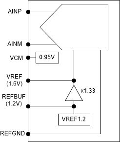
Note: The voltage reference mode can be selected using SPI writes or by using the REFBUF pin (default) as a control pin (Configuration using PINs only). If the REFBUF pin is not used for configuration, the REFBUF pin should be connected to AVDD (even though the REFBUF pin has a weak internal pullup to AVDD) and the voltage reference option has to be selected using the SPI interface.

GUID-D78E41C8-6E3B-4BD4-8784-419BF7F39F55-low.gifFigure 8-17 Different voltage reference options for ADC356x