ZHCSI83C may 2018 – may 2023 ADC12DL3200
PRODUCTION DATA
- 1
- 1特性
- 2应用
- 3说明
- 4Revision History
- 5Pin Configuration and Functions
-
6Specifications
- 6.1 Absolute Maximum Ratings
- 6.2 ESD Ratings
- 6.3 Recommended Operating Conditions
- 6.4 Thermal Information
- 6.5 Electrical Characteristics: DC Specifications
- 6.6 Electrical Characteristics: Power Consumption
- 6.7 Electrical Characteristics: AC Specifications (Dual-Channel Mode)
- 6.8 Electrical Characteristics: AC Specifications (Single-Channel Mode)
- 6.9 Timing Requirements
- 6.10 Switching Characteristics
- 6.11 Typical Characteristics
-
7Detailed Description
- 7.1 Overview
- 7.2 Functional Block Diagram
- 7.3
Feature Description
- 7.3.1 Analog Inputs
- 7.3.2 ADC Core
- 7.3.3 Timestamp
- 7.3.4 Clocking
- 7.3.5 LVDS Digital Interface
- 7.3.6 Alarm Monitoring
- 7.3.7 Temperature Monitoring Diode
- 7.3.8 Analog Reference Voltage
- 7.4
Device Functional Modes
- 7.4.1 Dual-Channel Mode (Non-DES Mode)
- 7.4.2 Internal Dither Modes
- 7.4.3 Single-Channel Mode (DES Mode)
- 7.4.4 LVDS Output Driver Modes
- 7.4.5 LVDS Output Modes
- 7.4.6 Power-Down Modes
- 7.4.7 Calibration Modes and Trimming
- 7.4.8 Offset Calibration
- 7.4.9 Trimming
- 7.5 Programming
- 7.6 Register Maps
- Application and Implementation
- 8Device and Documentation Support
- 9Mechanical, Packaging, and Orderable Information
封装选项
机械数据 (封装 | 引脚)
散热焊盘机械数据 (封装 | 引脚)
订购信息
7.3.4 Clocking
The clocking subsystem of the ADC12DL3200 has two input signals: the device clock (CLK+, CLK–) and SYSREF (SYSREF+, SYSREF–). Within the clocking subsystem there is a noiseless aperture delay adjustment (tAD adjust), a clock duty cycle corrector, and a SYSREF capture block. Figure 7-2 shows the clocking subsystem.
 Figure 7-2 ADC12DL3200 Clocking Subsystem
The device clock is used as the sampling clock for the ADC core as well as the clocking for the digital processing and LVDS outputs. Use a low-noise (low jitter) device clock to maintain high signal-to-noise ratio (SNR) within the ADC. In dual-channel mode, the analog input signal for each input is sampled on the rising edge of the device clock. In single-channel mode, both the rising and falling edges of the device clock are used to capture the analog signal to reduce the maximum clock rate required by the ADC. A noiseless aperture delay adjustment (tAD adjust) allows the sampling instance of the ADC to be shifted in fine steps in order to synchronize multiple ADC12DL3200 devices or to fine-tune system latency. Duty cycle correction is implemented in the ADC12DL3200 to ease the requirements on the external device clock while maintaining high performance. Table 7-3 summarizes the device clock interface in dual-channel mode and single-channel mode.
| MODE OF OPERATION | SAMPLING RATE VS fCLK | SAMPLING INSTANT |
|---|---|---|
| Dual-channel mode | 1 × fCLK | Rising edge |
| Single-channel mode | 2 × fCLK | Rising and falling edge |
SYSREF is a system timing reference used to reset clock dividers and strobe generation within the ADC12DL3200 that is similar to the SYSREF signal used by JESD204B interface devices. SYSREF is used to synchronize multiple ADC12DL3200 devices. SYSREF must be captured by the correct device clock edge in order to achieve repeatable latency and synchronization. The ADC12DL3200 includes SYSREF windowing and automatic SYSREF calibration to ease the requirements on the external clocking circuits and to simplify the synchronization process. SYSREF can be implemented as a single pulse or as a periodic clock. In periodic implementations, SYSREF must be equal to, or an integer division of, the frame clock frequency. Equation 2 can be used to calculate valid SYSREF frequencies.
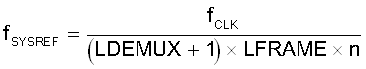
where
- LDEMUX and LFRAME are register settings
- fCLK is the device clock frequency (CLK±)
- n is any positive integer