ZHCSNM2A December   2021  – April 2022 ADC128S102-SEP

PRODUCTION DATA  

  1. 特性
  2. 应用
  3. 说明
  4. Revision History
  5. Pin Configuration and Functions
  6. Specifications
    1. 6.1 Absolute Maximum Ratings
    2. 6.2 ESD Ratings
    3. 6.3 Recommended Operating Conditions
    4. 6.4 Thermal Information
    5. 6.5 Electrical Characteristics
    6. 6.6 Timing Requirements
    7. 6.7 Switching Characteristics
    8. 6.8 Timing Diagrams
    9. 6.9 Typical Characteristics
  7. Detailed Description
    1. 7.1 Overview
    2. 7.2 Functional Block Diagram
    3. 7.3 Feature Description
      1. 7.3.1 ADC128S102-SEP Transfer Function
      2. 7.3.2 Analog Inputs
      3. 7.3.3 Digital Inputs and Outputs
      4. 7.3.4 Radiation Environments
        1. 7.3.4.1 Total Ionizing Dose
        2. 7.3.4.2 Single Event Latch-Up
    4. 7.4 Device Functional Modes
      1. 7.4.1 ADC128S102-SEP Operation
    5. 7.5 Programming
      1. 7.5.1 Serial Interface
  8. Application and Implementation
    1. 8.1 Application Information
    2. 8.2 Typical Application
      1. 8.2.1 Design Requirements
      2. 8.2.2 Detailed Design Procedure
      3. 8.2.3 Application Curve
  9. Power Supply Recommendations
    1. 9.1 Power-Supply Sequence
    2. 9.2 Power Management
    3. 9.3 Power-Supply Noise Considerations
  10. 10Layout
    1. 10.1 Layout Guidelines
    2. 10.2 Layout Example
  11. 11Device and Documentation Support
    1. 11.1 接收文档更新通知
    2. 11.2 支持资源
    3. 11.3 Trademarks
    4. 11.4 Electrostatic Discharge Caution
    5. 11.5 术语表
  12. 12Mechanical, Packaging, and Orderable Information
    1. 12.1 Engineering Samples

封装选项

机械数据 (封装 | 引脚)
散热焊盘机械数据 (封装 | 引脚)
订购信息

Typical Application

Figure 8-1 shows a typical application block diagram. The split analog and digital supply pins are both powered in this example by the Texas Instruments' LP2950-N low-dropout voltage regulator. The analog supply is bypassed with a capacitor network located close to the ADC128S102-SEP. The digital supply is separated from the analog supply by an isolation resistor and bypassed with additional capacitors. The ADC128S102-SEP uses the analog supply (VA) as its reference voltage; thus, VA must be kept as clean as possible. Because of the low power requirements of the ADC128S102-SEP, a precision reference can also be used as a power supply.
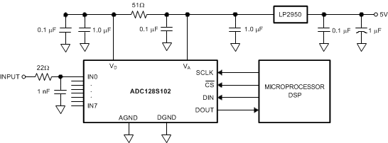
GUID-687E20C5-7B72-4ECF-887D-380D9DE5E3EF-low.gifFigure 8-1 Typical Application Circuit