ZHCSCU1 September 2014 TPS53632
PRODUCTION DATA.
- 1 特性
- 2 应用
- 3 说明
- 4 修订历史记录
- 5 Pin Configuration and Functions
- 6 Specifications
-
7 Detailed Description
- 7.1 Overview
- 7.2 Functional Block Diagram
- 7.3
Feature Description
- 7.3.1 Current Sensing
- 7.3.2 Load Transients
- 7.3.3 AutoBalance Current Sharing
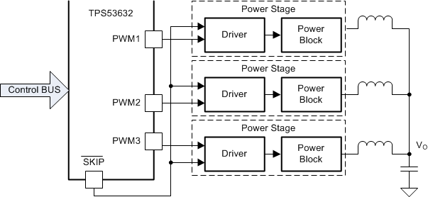
- 7.3.4 PWM and SKIP Signals
- 7.3.5 5-V, 3.3-V and 1.8-V Undervoltage Lockout (UVLO)
- 7.3.6 Output Undervoltage Protection (UVP)
- 7.3.7 Overcurrent Protection (OCP)
- 7.3.8 Overvoltage Protection
- 7.3.9 Analog Current Monitor, IMON and Corresponding Digital Output Current
- 7.3.10 Addressing
- 7.3.11 I2C Interface Operation
- 7.3.12 Start-Up Sequence
- 7.3.13 Phase Add and Drop Operation
- 7.3.14 Power Good Operation
- 7.3.15 Input Voltage Limits
- 7.3.16 Fault Behavior
- 7.4 Device Functional Modes
- 7.5 Configuration and Programming
- 7.6 Register Maps
-
8 Applications and Implementation
- 8.1 Application Information
- 8.2
Typical Application
- 8.2.1
3-Phase D-CAP+™, Step-Down Application
- 8.2.1.1 Design Requirements
- 8.2.1.2
Detailed Design Procedure
- 8.2.1.2.1 Step 1: Select Switching Frequency
- 8.2.1.2.2 Step 2: Set The Slew Rate
- 8.2.1.2.3 Step 3: Determine Inductor Value And Choose Inductor
- 8.2.1.2.4 Step 4: Determine Current Sensing Method
- 8.2.1.2.5 Step 5: DCR Current Sensing
- 8.2.1.2.6 Step 6: Select OCP Level
- 8.2.1.2.7 Step 7: Set the Load-Line Slope
- 8.2.1.2.8 Step 8: Current Monitor (IMON) Setting
- 8.2.1.3 Application Performance Plots
- 8.2.1.4 Loop Compensation for Zero Load-Line
- 8.2.1
3-Phase D-CAP+™, Step-Down Application
- 9 Power Supply Recommendations
- 10 Layout
- 11器件和文档支持
- 12机械封装和可订购信息
1 特性
- 可选相位数:(3,2 或 1)
- 针对 VID 控制和遥感勘测的 I2C 接口(具有 8 个器件地址)
- 针对快速瞬态响应提供 D-CAP+™ 控制
- 动态相位增加和下降操作
- 开关频率:300kHz 至 1MHz
- 数字电流监控
- 7 位数模转换器 (DAC) 输出范围:0.50V 至 1.52V
- 轻负载与重负载下实现最优效率
- 精确、可调电压定位或零斜率负载线路
- 已获专利 AutoBalance™ 相位均衡
- 可选 8 级电流限制
- 2.5V 至 24V 转换电压范围
- 默认启动电压:1.00V
- 小型 4mm x 4mm 32 引脚超薄四方扁平无引线 (VQFN) PowerPAD 封装
2 应用
- 高电流低压应用
- 微服务器的内核电源、定制微控制器、专用集成电路 (ASIC)
3 说明
TPS53632 器件是一款采用串行控制的降压无驱动器控制器。 具有 D-CAP+ 架构等高级特性,可实现快速瞬态响应、最低输出波纹和高效率。 TPS53632 器件支持标准 I2C Rev 3.0 接口,能够实现输出电压动态控制以及电流监视器遥测。 它还具有动态相位增加和下降控制功能,可进入单相断续电流模式,从而大大增加轻负载时的效率。
其它特性包括可调整控制 VCORE 转换率以及电压定位。 TPS51604 器件驱动器专门针对这一系列控制器而设计。 此外,TPS53632 器件还可配合德州仪器 (TI) 功率级器件(MOSFET 驱动器)使用。 TPS53632 器件采用节省空间的耐热增强型 32 引脚 VQFN 封装,额定工作温度范围为 –10°C 至 105°C。
器件信息
| 部件号 | 封装 | 封装尺寸 |
|---|---|---|
| TPS53632 | VQFN | 4mm x 4mm |
简化电路原理图