SBOS507A February 2010 – December 2014 TLV3502-Q1
PRODUCTION DATA.
1 Features
- Qualified for Automotive Applications
- AEC-Q100 Qualified With the Following Results:
- Device Temperature Grade 1: –40°C to +125°C Ambient Operating Temperature Range
- Device HBM ESD Classification Level 2
- Device CDM ESD Classification Level C4B
- High Speed: 4.5 ns
- Rail-To-Rail I/O
- Supply Voltage: 2.7 V To 5.5 V
- Push-Pull CMOS Output Stage
- Shutdown
- Micro Package: SOT23-8
- Low Supply Current: 3.2 mA
2 Applications
- HEV/EV, Powertrain, and Passive Safety:
- Threshold Detector
- Zero-Crossing Detector
- Window Comparator
- Oscillator
3 Description
The TLV3502-Q1 push-pull output comparators feature a fast 4.5-ns propagation delay and operation from 2.7 V to 5.5 V. Beyond-the-rails input common-mode range makes the device an ideal choice for low-voltage applications. The rail-to-rail output directly drives either CMOS or TTL logic.
A microsize package provides options for portable and space-restricted applications. The TLV3502-Q1 device is available in the SOT23-8 (DCN) package.
Device Information(1)
| PART NUMBER | PACKAGE | BODY SIZE (NOM) |
|---|---|---|
| TLV3502-Q1 | SOT-23 (8) | 2.90 mm × 1.60 mm |
- For all available packages, see the orderable addendum at the end of the datasheet.
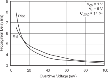
Propagation Delay vs Overdrive Voltage