SBOS507A February 2010 – December 2014 TLV3502-Q1
PRODUCTION DATA.
6 Specifications
6.1 Absolute Maximum Ratings
over operating free-air temperature range (unless otherwise noted) (1)| MIN | MAX | UNIT | ||
|---|---|---|---|---|
| Supply voltage | 5.5 | V | ||
| Signal input terminal voltage(2) | (V−) − 0.3 | (V+) + 0.3 | V | |
| Signal input terminal current(2) | 10 | mA | ||
| Output short-circuit current(3) | 74 | mA | ||
| Thermal impedance, junction to free air | 200 | 200 | °C/W | |
| Operating temperature | −40 | 125 | °C | |
| Junction temperature | 150 | °C | ||
| Storage temperature, Tstg | −65 | 150 | °C | |
(1) Stresses beyond those listed under Absolute Maximum Ratings may cause permanent damage to the device. These are stress ratings only, which do not imply functional operation of the device at these or any other conditions beyond those indicated under Recommended Operating Conditions. Exposure to absolute-maximum-rated conditions for extended periods may affect device reliability.
(2) Input terminals are diode-clamped to the power-supply rails. Input signals that can swing more than 0.3 V beyond the supply rails should be current limited to 10mA or less.
(3) Short circuit to ground, one comparator per package
6.2 ESD Ratings
| VALUE | UNIT | |||||
|---|---|---|---|---|---|---|
| V(ESD) | Electrostatic discharge | Human body model (HBM), per AEC Q100-002(1) | ±2000 | V | ||
| Charged device model (CDM), per AEC Q100-011 | Corner pins (+IN A, –IN B, V+, and V–) | ±750 | ||||
| Other pins | ±500 | |||||
(1) AEC Q100-002 indicates HBM stressing is done in accordance with the ANSI/ESDA/JEDEC JS-001 specification.
6.3 Recommended Operating Conditions
over operating free-air temperature range (unless otherwise noted)| MIN | NOM | MAX | UNIT | ||
|---|---|---|---|---|---|
| VS | Supply voltage | 2.2 | 2.7 | 5.5 | V |
| VIL | Low-level input voltage, shutdown (comparator is enabled)(2) | (V+) - 1.7 | V | ||
| VIH | High-level input voltage, shutdown (comparator is disabled)(2) | (V+) – 0.9 | V | ||
| TA | Operating temperature | –40 | 125 | °C | |
(1) Measured between 10% of VS and 90% of VS.
(2) When the shutdown pin is within 0.9 V of the most positive supply, the part is disabled. When it is more than 1.7 V below the most positive supply, the part is enabled.
6.4 Thermal Information
| THERMAL METRIC(1) | TLV3502-Q1 | UNIT | |
|---|---|---|---|
| SOT-23 | |||
| 8 PINS | |||
| RθJA | Junction-to-ambient thermal resistance | 191.6 | °C/W |
| RθJC(top) | Junction-to-case (top) thermal resistance | 43.9 | |
| RθJB | Junction-to-board thermal resistance | 120.3 | |
| ψJT | Junction-to-top characterization parameter | 14.4 | |
| ψJB | Junction-to-board characterization parameter | 118.6 | |
(1) For more information about traditional and new thermal metrics, see the IC Package Thermal Metrics application report, SPRA953.
6.5 Electrical Characteristics
TA = 25°C and VS = 2.7 V to 5.5 V (unless otherwise noted)| PARAMETER | TEST CONDITIONS | MIN | TYP | MAX | UNIT | |
|---|---|---|---|---|---|---|
| VOS | Input offset voltage(1) | VCM = 0 V, IO = 0 mA | ±1 | ±6.5 | mV | |
| ΔVOS/ΔT | Offset voltage vs temperature | TA = –40°C to 125°C | ±5 | µV/°C | ||
| PSRR | Offset voltage vs power supply | VS = 2.7 V to 5.5 V | 100 | 400 | µV/V | |
| Input hysteresis | 6 | mV | ||||
| IB | Input bias current | VCM = VCC/2, ΔVIN = ±5.5 V | ±2 | ±10 | pA | |
| IOS | Input offset current(2) | VCM = VCC/2, ΔVIN = ±5.5 V | ±2 | ±10 | pA | |
| VCM | Common-mode voltage range | (V–) - 0.2 | (V+) + 0.2 | V | ||
| CMRR | Common-mode rejection | VCM = –0.2 V to (V+) + 0.2 V | 57 | 70 | dB | |
| TA = −40°C to 125°C VCM = –0.2 V to (V+) + 0.2 V |
55 | |||||
| Common-mode input impedance | 1013 || 2 | Ω || pF | ||||
| Differential input impedance | 1013 || 4 | Ω || pF | ||||
| VOH | High-level voltage output from rail | IOUT = ±1 mA | 30 | 50 | mV | |
| VOL | Low-level voltage output from rail | IOUT = ±1 mA | 30 | 50 | mV | |
| Input bias current of shutdown pin | 2 | pA | ||||
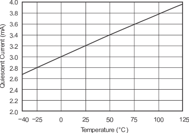
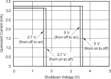
| IQ | Quiescent current per comparator | VS = 5 V, VO = High | 3.2 | 5 | mA | |
| IQ(SD) | Quiescent current in shutdown | 2 | µA | |||
(1) VOS is defined as the average of the positive and the negative switching thresholds.
(2) The difference between IB+ and IB−.
6.6 Switching Characteristics
TA = 25°C and VS = 2.7 V to 5.5 V (unless otherwise noted)| PARAMETER | TEST CONDITIONS | MIN | TYP | MAX | UNIT | |
|---|---|---|---|---|---|---|
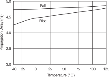
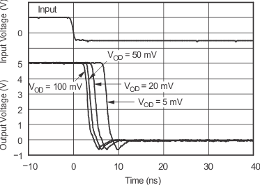
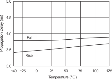
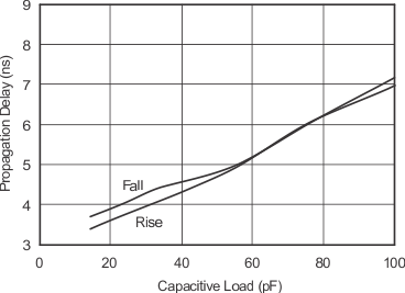
| tpd | Propagation delay time(1)(3) | ΔVIN = 100 mV, Overdrive = 20 mV | 4.5 | 6.4 | ns | |
| TA = −40°C to 125°C ΔVIN = 100 mV, Overdrive = 20 mV |
7 | ns | ||||
| ΔVIN = 100 mV, Overdrive = 5 mV | 7.5 | 10 | ns | |||
| TA = −40°C to 125°C ΔVIN = 100 mV, Overdrive = 5 mV |
12 | ns | ||||
| Δt(SKEW) | Propagation delay skew(2) | ΔVIN = 100 mV, Overdrive = 20 mV | 0.5 | ns | ||
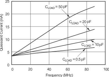
| fMAX | Maximum toggle frequency | Overdrive = 50 mV, VS = 5 V | 80 | MHz | ||
| tR | Rise time(1) | 1.5 | ns | |||
| tF | Fall time(1) | 1.5 | ns | |||
| tOFF | Shutdown turn-off time | 30 | ns | |||
| tON | Shutdown turn-on time | 100 | ns | |||
(1) Propagation delay cannot be accurately measured with low overdrive on automatic test equipment. This parameter is ensured by characterization at 100-mV overdrive.
(2) The difference between the propagation delay going high and the propagation delay going low.
(3) Not production tested
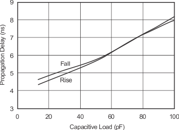
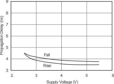
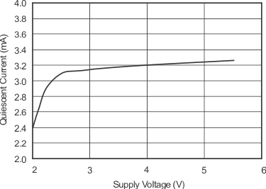
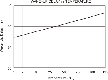
6.7 Typical Characteristics
TA = 25°C, VS = 5 V, Input Overdrive = 100 mV (unless otherwise noted)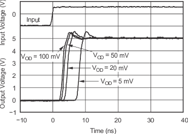
| VOD = 20 mV |
| VOD = 20 mV |
| VDD = 5 V | VIN = 20 mVpp |
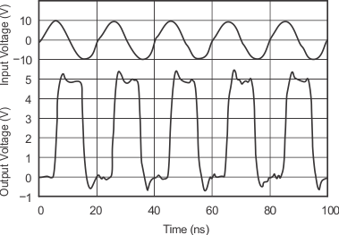
| VDD = 5 V | VIN = 20 mVpp |
| VOD = 50 mV |
| VOD = 50 mV |
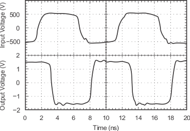
| ±2.5-V dual supply into 50-Ω oscilloscope input |