SBOS507A February 2010 – December 2014 TLV3502-Q1
PRODUCTION DATA.
8 Application and Implementation
NOTE
Information in the following applications sections is not part of the TI component specification, and TI does not warrant its accuracy or completeness. TI’s customers are responsible for determining suitability of components for their purposes. Customers should validate and test their design implementation to confirm system functionality.
8.1 Application Information
The TLV3502-Q1 device features high-speed response and includes 6 mV of internal hysteresis for improved noise immunity with an input common-mode range that extends 0.2 V beyond the power-supply rails.
8.2 Typical Application
In this example, we will show how can we add external hysteresis to TLV3502-Q1 device to achieve greater noise immunity. First, let's understand when and why external hysteresis may be required.
The TLV3502-Q1 device has a robust performance when used with a good layout. However, comparator inputs have little noise immunity within the range of specified offset voltage (±5 mV). For slow moving or noisy input signals, the comparator output may display multiple switching as input signals move through the switching threshold. In such applications, the 6mV of internal hysteresis of the TLV3502-Q1 device might not be sufficient. In cases where greater noise immunity is desired, external hysteresis may be added by connecting a small amount of feedback to the positive input.
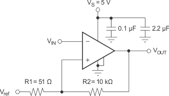 Figure 19. Application Adding Hysteresis to the TLV350x
8.2.1 Design Requirements
Figure 19 shows a typical topology used to introduce 25 mV of additional hysteresis, for a total of 31-mV hysteresis when operating from a single 5-V supply.
8.2.2 Detailed Design Procedure
Use Equation 1 to calculate the total hysteresis.
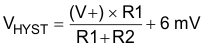
VHYST sets the value of the transition voltage required to switch the comparator output by enlarging the threshold region, thereby reducing sensitivity to noise.
8.2.3 Application Curve
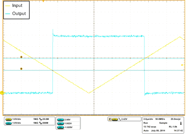 Figure 20. TLV3502 With Upper and Lower Threshold With 1-V Hysteresis