ZHCSJK9H June 2001 – October 2015 TPS54610
PRODUCTION DATA.
- 1 特性
- 2 应用
- 3 说明
- 4 修订历史记录
- 5 Device Comparison Table
- 6 Pin Configuration and Functions
- 7 Specifications
-
8 Detailed Description
- 8.1 Overview
- 8.2 Functional Block Diagram
- 8.3
Feature Description
- 8.3.1 Undervoltage Lockout (UVLO)
- 8.3.2 Slow Start/Enable (SS/ENA)
- 8.3.3 VBIAS Regulator (VBIAS)
- 8.3.4 Voltage Reference
- 8.3.5 Oscillator and PWM Ramp
- 8.3.6 Error Amplifier
- 8.3.7 PWM Control
- 8.3.8 Dead-Time Control and MOSFET Drivers
- 8.3.9 Overcurrent Protection
- 8.3.10 Thermal Shutdown
- 8.3.11 Power-Good (PWRGD)
- 8.4 Device Functional Modes
- 9 Application and Implementation
- 10Power Supply Recommendations
- 11Layout
- 12器件和文档支持
- 13机械、封装和可订购信息
11.3 Thermal Considerations
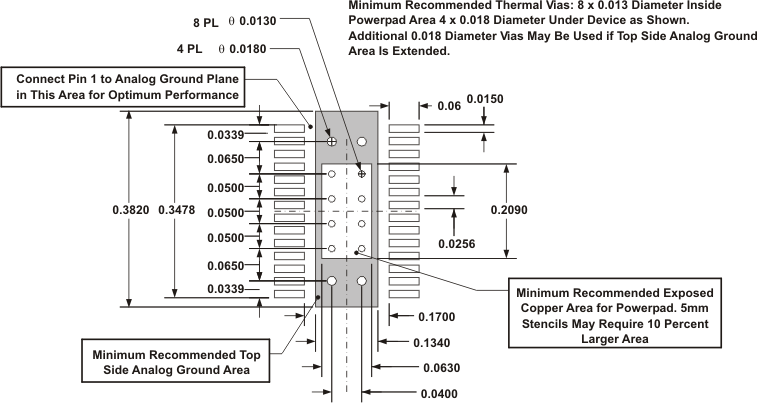
For operation at full rated load current, the analog ground plane must provide an adequate heat dissipating area. A 3-inch by 3-inch plane of 1 ounce copper is recommended, though not mandatory, depending on ambient temperature and airflow. Most applications have larger areas of internal ground plane available, and the PowerPAD™ must be connected to the largest area available. Additional areas on the top or bottom layers also help dissipate heat, and any area available must be used when 6 A or greater operation is desired. Connection from the exposed area of the PowerPAD™ to the analog ground plane layer must be made using 0.013 inch diameter vias to avoid solder wicking through the vias. Eight vias must be in the PowerPAD area with four additional vias located under the device package. The size of the vias under the package, but not in the exposed thermal pad area, can be increased to 0.018. Additional vias beyond the twelve recommended that enhance thermal performance must be included in areas not under the device package.
 Figure 23. Recommended Land Pattern for 28-Pin PWP PowerPAD