ZHCSJK9H June   2001  – October 2015 TPS54610

PRODUCTION DATA.  

  1. 特性
  2. 应用
  3. 说明
    1.     Device Images
      1.      简化原理图
      2.      在 350 kHz 时的效率
  4. 修订历史记录
  5. Device Comparison Table
  6. Pin Configuration and Functions
    1.     Pin Functions
  7. Specifications
    1. 7.1 Absolute Maximum Ratings
    2. 7.2 ESD Ratings
    3. 7.3 Recommended Operating Conditions
    4. 7.4 Thermal Information
    5. 7.5 Electrical Characteristics
    6. 7.6 Dissipation Ratings
    7. 7.7 Typical Characteristics
  8. Detailed Description
    1. 8.1 Overview
    2. 8.2 Functional Block Diagram
    3. 8.3 Feature Description
      1. 8.3.1  Undervoltage Lockout (UVLO)
      2. 8.3.2  Slow Start/Enable (SS/ENA)
      3. 8.3.3  VBIAS Regulator (VBIAS)
      4. 8.3.4  Voltage Reference
      5. 8.3.5  Oscillator and PWM Ramp
      6. 8.3.6  Error Amplifier
      7. 8.3.7  PWM Control
      8. 8.3.8  Dead-Time Control and MOSFET Drivers
      9. 8.3.9  Overcurrent Protection
      10. 8.3.10 Thermal Shutdown
      11. 8.3.11 Power-Good (PWRGD)
    4. 8.4 Device Functional Modes
      1. 8.4.1 Continuous Conduction Mode
      2. 8.4.2 Switching Frequency Selection/Synchronization
  9. Application and Implementation
    1. 9.1 Application Information
    2. 9.2 Typical Applications
      1. 9.2.1 High Frequency Switching Regulator Using Ceramic Output Capacitors
        1. 9.2.1.1 Design Requirements
        2. 9.2.1.2 Detailed Design Procedure
          1. 9.2.1.2.1 Component Selection
          2. 9.2.1.2.2 Input Filter
          3. 9.2.1.2.3 Feedback Circuit
          4. 9.2.1.2.4 Operating Frequency
          5. 9.2.1.2.5 Output Filter
        3. 9.2.1.3 Application Curves
      2. 9.2.2 High Frequency Application
        1. 9.2.2.1 Design Requirements
        2. 9.2.2.2 Detailed Design Procedure
        3. 9.2.2.3 Application Curve
  10. 10Power Supply Recommendations
  11. 11Layout
    1. 11.1 Layout Guidelines
    2. 11.2 Layout Example
    3. 11.3 Thermal Considerations
  12. 12器件和文档支持
    1. 12.1 器件支持
      1. 12.1.1 相关直流/直流产品
    2. 12.2 接收文档更新通知
    3. 12.3 社区资源
    4. 12.4 商标
    5. 12.5 静电放电警告
    6. 12.6 术语表
  13. 13机械、封装和可订购信息

Typical Characteristics

TPS54610 G001_slvsar4.gif
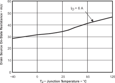
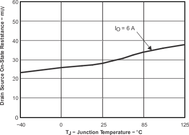
VIN = 3.3 V
Figure 1. Drain-Source On-State Resistance vs
Junction Temperature
TPS54610 G003_slvsar4.gif
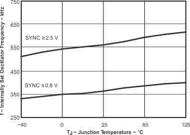
Figure 3. Internally Set Oscillator Frequency vs
Junction Temperature
TPS54610 G005_slvsar4.gif
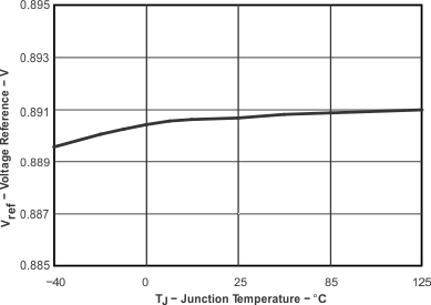
Figure 5. Voltage Reference vs Junction Temperature
TPS54610 G007_slvsar4.gif
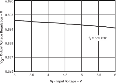
TJ = 85°C IO = 3 A
Figure 7. Output Voltage Regulation vs Input Voltage
TPS54610 G009_slvsar4.gif
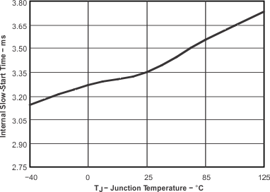
Figure 9. Internal Slow-Start Time vs Junction Temperature
TPS54610 G002_slvsar4.gif
VIN = 5 V
Figure 2. Drain-Source On-State Resistance vs
Junction Temperature
TPS54610 G004_slvsar4.gif
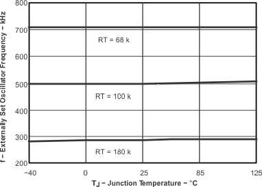
Figure 4. Externally Set Oscillator Frequency vs
Junction Temperature
TPS54610 G006_slvsar4.gif
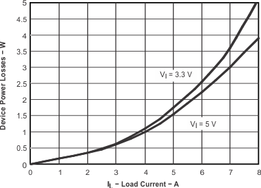
TJ = 125°C fs = 700 kHz
Figure 6. Device Power Losses at TJ = 125°C vs
Load Current
TPS54610 G008_slvsar4.gif
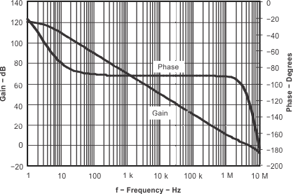
RL= 10 kΩ CL = 160 pF TA = 25°C
Figure 8. Error Amplifier Open Loop Response