ZHCSHN1A August   2017  – February 2018 UCC24612

PRODUCTION DATA.  

  1. 特性
  2. 应用
  3. 说明
    1.     Device Images
      1.      具有高侧 SR 的反激式
      2.      具有低侧 SR 的反激式
  4. 修订历史记录
  5. Pin Configuration and Functions
    1.     Pin Functions
  6. Specifications
    1. 6.1 Absolute Maximum Ratings
    2. 6.2 ESD Ratings
    3. 6.3 Recommended Operating Conditions
    4. 6.4 Thermal Information
    5. 6.5 Electrical Characteristics
    6. 6.6 Timing Requirements
    7. 6.7 Typical Characteristics
  7. Detailed Description
    1. 7.1 Overview
    2. 7.2 Functional Block Diagram
    3. 7.3 Feature Description
      1. 7.3.1 Power Management
      2. 7.3.2 Synchronous Rectifier Control
      3. 7.3.3 Adaptive Blanking Time
        1. 7.3.3.1 Turn-On Blanking Timer (Minimum On Time)
        2. 7.3.3.2 Turn-Off Blanking Timer
        3. 7.3.3.3 SR Turn-on Re-arm
      4. 7.3.4 Gate Voltage Clamping
      5. 7.3.5 Standby Mode
    4. 7.4 Device Functional Modes
      1. 7.4.1 UVLO Mode
      2. 7.4.2 Standby Mode
      3. 7.4.3 Run Mode
  8. Application and Implementation
    1. 8.1 Application Information
    2. 8.2 Typical Application
      1. 8.2.1 Design Requirements
      2. 8.2.2 Detailed Design Procedure
        1. 8.2.2.1 SR MOSFET Selection
        2. 8.2.2.2 Bypass Capacitor Selection
        3. 8.2.2.3 Snubber design
        4. 8.2.2.4 High-Side Operation
      3. 8.2.3 Application Curves
        1. 8.2.3.1 Steady State Testing Low-Side Configuration
        2. 8.2.3.2 Steady State Testing High-Side Configuration
  9. Power Supply Recommendations
  10. 10PCB Layout
    1. 10.1 Layout Guidelines
    2. 10.2 Layout Example
  11. 11器件和文档支持
    1. 11.1 社区资源
    2. 11.2 商标
    3. 11.3 静电放电警告
    4. 11.4 Glossary
  12. 12机械、封装和可订购信息

Typical Characteristics

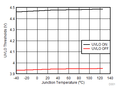
UCC24612 D017_SLUSCM5.gifFigure 1. UVLO Threshold Voltage vs Temperature
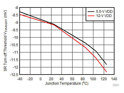
UCC24612 D031_SLUSCM5.gifFigure 3. SR Turn-off Threshold Voltages vs Temperature
UCC24612 D021_SLUSCM5.gif
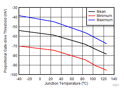
Figure 5. Proportional Gate-drive Threshold vs Temperature
UCC24612 D023_SLUSCM5.gif
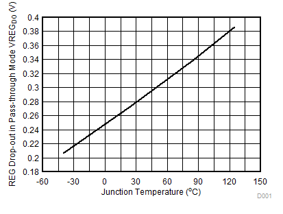
Figure 7. REG Drop-out in Pass-through Mode vs Temperature, ILOAD_REG = 10 mA
UCC24612 D025_SLUSCM5.gif
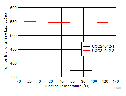
Figure 9. Turn-On Blanking Time vs Temperature
UCC24612 D028_SLUSCM5.gif
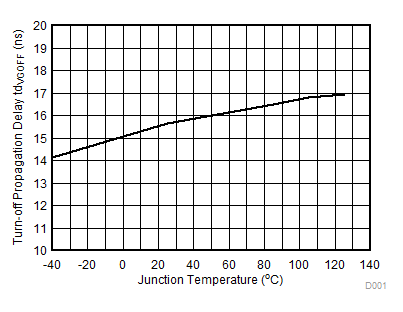
Figure 11. SR Turn-off Propagation Delay vs Temperature
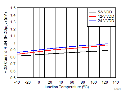
UCC24612 D018_SLUSCM5.gifFigure 2. Bias Supply Current vs. Temperature (CVG= 0 pF, VVD = 1 V and No Switching)
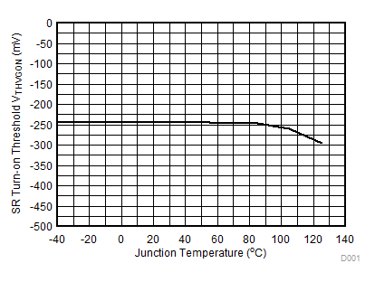
UCC24612 D020_SLUSCM5.gifFigure 4. SR Turn-on Threshold Voltage vs Temperature
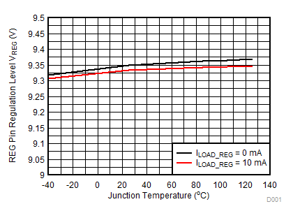
UCC24612 D026_SLUSCM5.gif
Figure 6. REG Pin Voltage vs Temperature at Different Loading Conditions
UCC24612 D030_SLUSCM5.gif
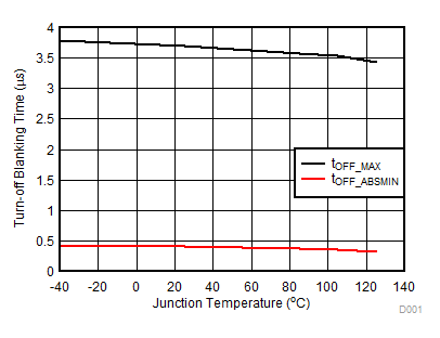
Figure 8. Abs. Minimum Turn-off Blanking Time and Maximum Turn-off Blanking Time vs Temperature
UCC24612 D027_SLUSCM5.gif
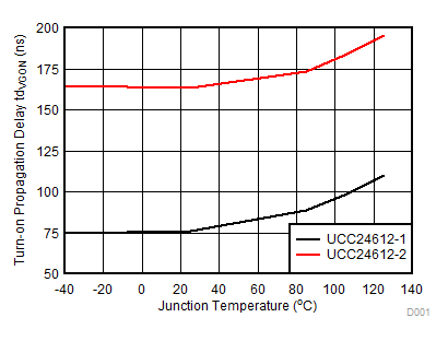
Figure 10. SR Turn-on Delay Time vs Temperature
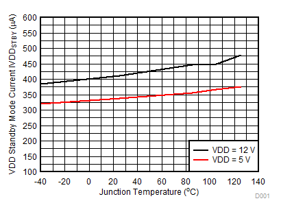
UCC24612 D029_SLUSCM5.gif
Figure 12. Standby Current vs Temperature