SWRU437B September 2015 – June 2020 WL1801MOD , WL1805MOD , WL1807MOD , WL1831MOD , WL1835MOD , WL1837MOD
6 Antenna
This device is intended only for OEM integrators under the following conditions:
- The antenna must be installed so that 20 cm is maintained between the antenna and users.
- The transmitter module cannot be co-located with any other transmitter or antenna.
- The radio transmitter can operate only using an antenna of a type and maximum (or lesser) gain approved by TI. Table 5 lists the antennas approved by TI for use with the radio transmitter along with maximum allowable gain values. Antenna types not included in the list or having a gain greater than the maximum indicated are strictly prohibited for use with this transmitter.
Table 5. Approved Antenna Types and Maximum Gain Values
| Antenna Type | Brand | 2.4 GHz | 4.9 to 5.9 GHz (1) | Unit |
|---|---|---|---|---|
| PCB | Ethertronics | –0.600 | 4.50 | dBi |
| Dipole | LSR | 2.00 | 2.00 | |
| PCB | Laird | 2.00 | 4.00 | |
| Chip | Pulse | 3.20 | 4.20 | |
| PIFA | LSR | 2.00 | 3.00 | |
| Chip | TDK | 2.27 | 3.96 |
- Range is approximate.
NOTE
If these conditions cannot be met (for example, with certain laptop configurations or co-location with another transmitter), the FCC/IC authorization will not be considered valid and the FCC ID/IC ID cannot be used on the final product. In these circumstances, the OEM integrator is responsible for reevaluating the end product (including the transmitter) and obtaining a separate FCC/IC authorization.
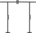
- It is suggested to place a Pi matching network place holder before the antenna on board
- It is strongly advised to have a debug miniature connector on the PCB
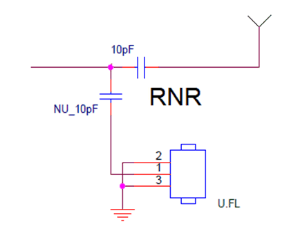
- Switching between the antenna and the debug connector should be done in RNR configuration to avoid stubs
- Antenna should be placed away from the rest of the circuit
- Avoid digital and analog routing in the area, metal enclosure.
- MIMO antenna spacing
- Distance between the two antennas is advised to be greater than half of the wavelength (62.5 mm at 2.4 GHz)
 Figure 5. Antenna Matching Network in PI Configuration
  Figure 6. RNR Configuration