SSZT705 may 2018 LM5109B , UCC27710 , UCC27712
While commuting to work, waiting for a traffic light I noticed the green and red light sequence that prevents traffic flow conflicts, or crashes. The crossing traffic directions are out of sequence to ensure safe driving. Also the yellow gives a little extra time to ensure everything runs smoothly.
In a half bridge power train, such as in DC drives, it is important to make sure there are no timing conflicts between the high and low-side power devices. Like with the yellow light, there needs to be some time to make sure the power devices are not on at the same time during the switching transitions.
When selecting a gate driver for your DC drives, there are design details to consider in order to achieve higher system robustness. In part 1 of this series (How to achieve higher system robustness in DC drives part 1: negative voltage) German Aguirre discussed negative voltage spikes on the switch-node HS pin. In part 2, I’ll discuss output interlock and deadtime.
Output interlock is a feature that prevents the outputs (LO and HO) from being high at the same time, even if the inputs (LI and HI) are both high. This prevents a potentially destructive shoot-through condition in the half-bridge. To ensure that both metal-oxide semiconductor field-effect transistors (MOSFETs) cannot be on at the same time, there may be a minimum deadtime feature so that one MOSFET can switch off completely before the other switches on.
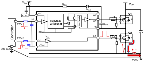
One common problem in motor control is voltage spikes and ringing on the driver input signals caused by parasitic layout inductance. Figure 1 shows the board layout trace inductances that exist in any design. These parasitic inductances should be minimized, but can never be eliminated, so a well-suited gate driver handles the transients they cause.
The red arrows in Figure 1 show an example of low-side turn on during hard switching operation: the falling VDS voltage generates a current spike upon discharge of the switch node capacitance. This high dI/dt current spike will generate a voltage because of the parasitic source inductance on the MOSFET and printed circuit board (PCB) traces. As the driver ground (COM) is typically connected close to the MOSFET source, and the controller is usually connected to a quiet ground such as the input capacitor, this voltage spike can appear on the MOSFET driver inputs.
 Figure 1 Driver Input Voltage
Spikes/ringing from Layout Inductance
Figure 1 Driver Input Voltage
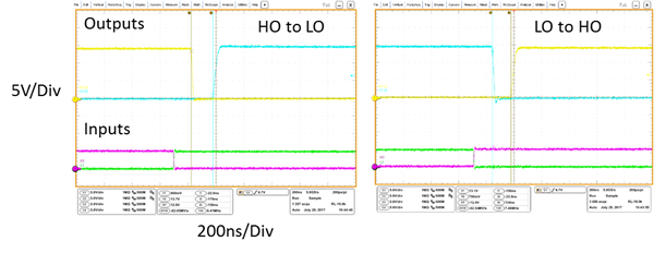
Spikes/ringing from Layout InductanceIt’s important that gate drivers have features that can tolerate voltage spikes in order to ensure reliable operation and improve robustness in your designs. The UCC27710 600V driver’s interlock feature prevents the LO and HO outputs from being high at the same time, and guarantees 150-ns of deadtime between the LO and HO outputs, as shown in Figure 2. This feature will ensure that the power MOSFETs will not have an unexpected cross conduction condition caused by noise on the driver inputs.
 Figure 2 LO and HO Deadtime with No LI
and HI Deadtime
Figure 2 LO and HO Deadtime with No LI
and HI DeadtimeLet’s discuss ways to reduce voltage spikes on the driver inputs. The first recommendation is the same as in part 1 of this series; reducing the parasitic inductance from the board layout. The layout of half-bridge power devices can be tight, what about the trace from the FET to the bulk input capacitor?
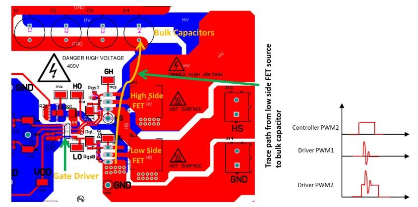
Figure 3 shows an example half-bridge driver and power-train layout. You can see that the MOSFETs are close together, but due to capacitor size, the bulk capacitor is often placed far from the FETs. This board layout path will result in significant source-to-capacitor parasitic inductance, which can result in large voltage spikes.
 Figure 3 Board Layout Path Resulting in
Parasitic Inductance
Figure 3 Board Layout Path Resulting in
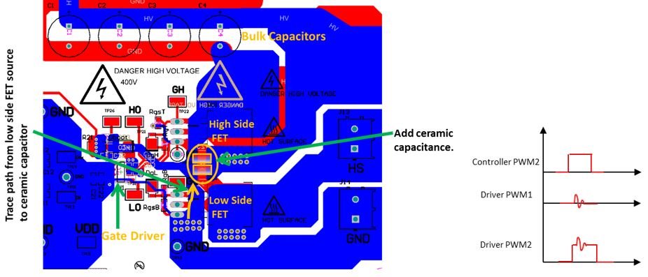
Parasitic InductanceFigure 4 shows the bottom layer of the same board layout. If you add high-voltage ceramic capacitors, you can place them very close to the power MOSFETs, significantly reducing the path from the low-side MOSFET source to the capacitor. Assuming that the parasitic inductance is relative to the path length, you can reduce the voltage spikes, as Figure 4 illustrates.
 Figure 4 Improved Board Layout
Resulting in a Reduced Voltage Spike
Figure 4 Improved Board Layout
Resulting in a Reduced Voltage SpikeThe second recommendation is to place a small resistor-capacitor (RC) filter on the driver inputs, as shown in Figure 5. The filter capacitor should be placed close to the driver and referenced to the COM pin.
 Figure 5 Driver Input RC Filter Placed
Close to the Driver
Figure 5 Driver Input RC Filter Placed
Close to the DriverInterlock and minimum deadtime are critical functions for gate drivers. Keep these concerns in mind to achieve higher system robustness when designing motor-drive applications.
Additional Resources
- These designs from the TI Designs library showcase robust gate drivers in DC drive and appliance subsystems:
- 230-V, 400-W 92% Efficiency Battery Charger with PFC and LLC for 36V Power Tools Reference Design.
- Electronically Commutated Motor Reference Design for HVAC Blowers with Low BOM Cost.
- 480W, 97% n Efficiency, Ultra-Compact (480W/in3), Bidirectional DC/DC Reference Design.
- 230V, 3.5kW PFC with >98% Efficiency Optimized for BOM and Size Reference Design.
- These TI gate driver products are robust candidates for DC drive applications: