SNVA881 November 2019 LP87521-Q1 , LP87522-Q1 , LP87523-Q1 , LP87524-Q1 , LP87525-Q1 , LP87561-Q1 , LP87562-Q1 , LP87563-Q1 , LP87564-Q1 , LP87565-Q1
5.1 Simulation Model
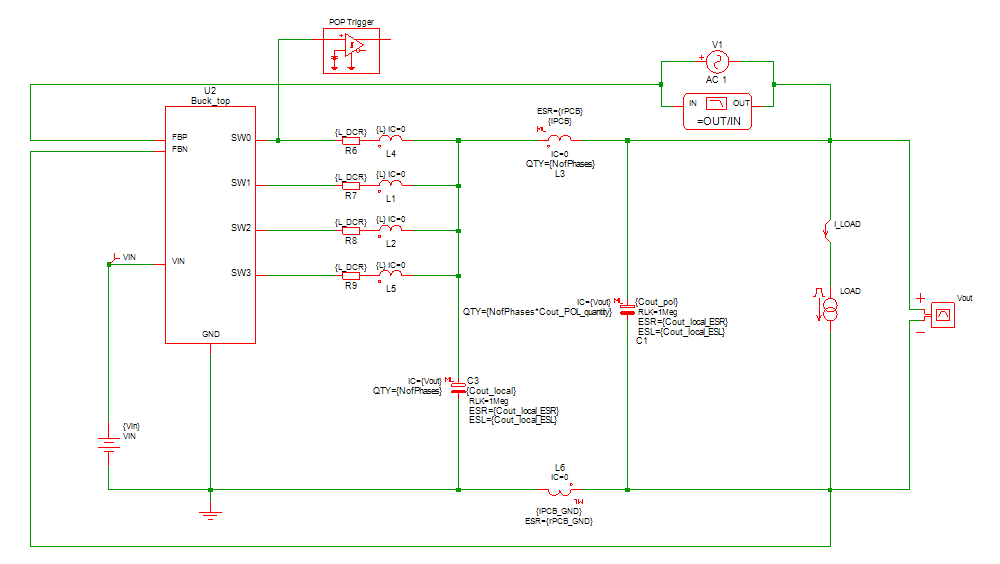
Simulations were completed using the simulation model schematic in Figure 6. The simulation model is available here. The model includes parameters for phase configuration, input and output voltage, switching frequency, local capacitance, and point of load capacitance. The model also has some of the parasitics parametrized, including the equivalent series inductances and resistances of capacitors, DC resistances of inductors, and PCB parasitics. To change these parameters press F11 to open the command window where the parameters are listed in a text format. Parameters and their descriptions are in Table 7.
Table 7. Simulation parameters
| Parameter | Description |
|---|---|
| Vin | Input voltage |
| Vout | Target output voltage |
| stepLow | Initial current in transient analysis |
| stepHigh | Pulse current in transient analysis |
| riseTime | Rise time of the pulse current |
| fallTime | Fall time of the pulse current |
| swFreq | Switching frequency |
| NofPhases | Phase count |
| Cout_local | Local capacitance per phase |
| Cout_local_ESR | Equivalent series resistance (ESR) of a local capacitor |
| Cout_local_ESL | Equivalent series inductance (ESL) of a local capacitor |
| Cout_local_shunt | Shunt resistance of local capacitor's ESL |
| Cout_POL | Point of load (POL) capacitance per phase |
| Cout_POL_ESR | Equivalent series resistance (ESR) of a POL capacitor |
| Cout_POL_ESL | Equivalent series inductance (ESL) of a POL capacitor |
| Cout_POL_quantity | POL capacitor quantity per phase |
| Cout_POL_shunt | Shunt resistance of POL capacitor's ESL |
| L | Inductor per phase |
| L_DCR | Inductor's DC resistance |
| rPCB | Parasitic resistance from PCB |
| lPCB | Parasitic inductance from PCB |
| rPCB_GND | Parasitic resistance from PCB ground plane |
| lPCB_GND | Parasitic inductance from PCB ground plane |
The capacitor parameters should be chosen according to the capacitance needed per phase. The simulation model provides Bode plot and step load transient simulation results when using the default simulation configuration. The step load parameters can be configured by double clicking the LOAD current waveform generator. The default configuration is step load of 1 A - 3 A - 1 A.
 Figure 6. Simulation schematic