SNVA881 November 2019 LP87521-Q1 , LP87522-Q1 , LP87523-Q1 , LP87524-Q1 , LP87525-Q1 , LP87561-Q1 , LP87562-Q1 , LP87563-Q1 , LP87564-Q1 , LP87565-Q1
4.2 Measurement Results
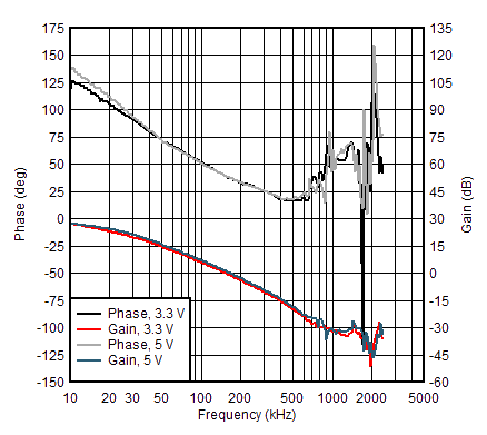
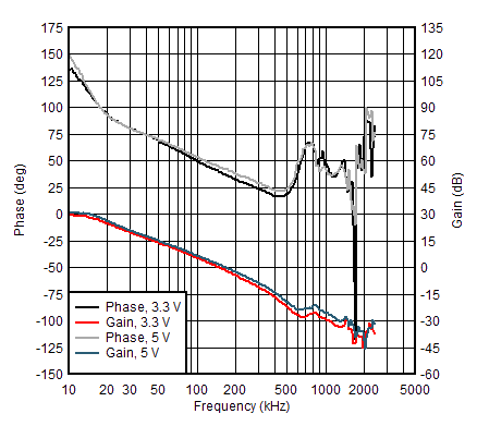
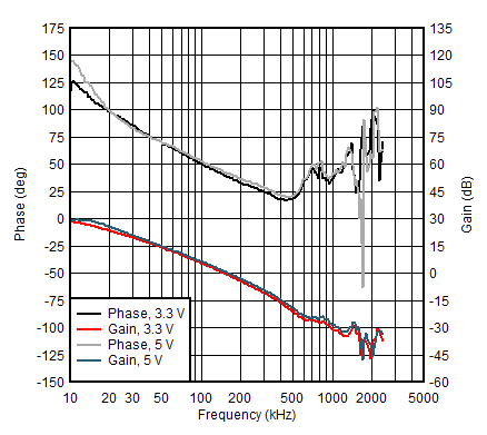
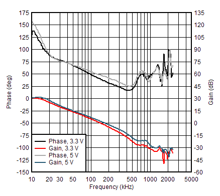
Typical Bode diagrams for every phase configuration are shown in Figure 2, Figure 3, Figure 4 and Figure 5. Each configuration has 1000 mV output voltage and 44 µF POL capacitance.
 Figure 2. VOUT=1000 mV, CPOL=44 µF/phase, 1-phase configuration
 Figure 4. VOUT=1000 mV, CPOL=44 µF/phase, 3-phase configuration
 Figure 3. VOUT=1000 mV, CPOL=44 µF/phase, 2-phase configuration
 Figure 5. VOUT=1000 mV, CPOL=44 µF/phase, 4-phase configuration
All measurement results are listed in Table 3, Table 4, Table 5 and Table 6 for each phase configuration. Results marked with N/A were not possible to measure due to the limitations in the measurement hardware as mentioned in Section 4.1. These results can be used when selecting point of load capacitance to fulfill phase margin requirements on specific VIN and VOUT.
Table 3. Measured gain and phase margins for 1-phase configuration
| VIN (V) | VOUT (mV) | CPOL (µF/phase) | Bandwidth (kHz) | Gain margin (dB) | Phase margin (deg) |
|---|---|---|---|---|---|
| 3.3 | 860 | 22 | 193.2 | 18.3 | 30.3 |
| 44 | 147.7 | 31.1 | 36.9 | ||
| 91 | 101.7 | 38.5 | 48.5 | ||
| 1000 | 22 | 201.2 | 17.8 | 32.0 | |
| 44 | 152.4 | 35.3 | 39.1 | ||
| 91 | 104.4 | N/A | 50.4 | ||
| 1800 | 22 | 224.5 | 17.3 | 38.8 | |
| 44 | 167.4 | 29.2 | 46.0 | ||
| 91 | 116.2 | 36.1 | 55.3 | ||
| 5.0 | 860 | 22 | 229.6 | 19.6 | 34.0 |
| 44 | 172.0 | N/A | 41.0 | ||
| 91 | 114.6 | N/A | 52.0 | ||
| 1000 | 22 | 219.0 | 19.9 | 30.8 | |
| 44 | 164.7 | N/A | 37.5 | ||
| 91 | 112.1 | N/A | 48.4 | ||
| 1800 | 22 | 245.7 | 17.7 | 39.2 | |
| 44 | 181.4 | 30.9 | 45.4 | ||
| 91 | 124.9 | 39.4 | 55.4 | ||
| 3300 | 22 | 296.9 | 13.8 | 45.4 | |
| 44 | 207.5 | 26.9 | 51.9 | ||
| 91 | 152.5 | 26.2 | 58.1 |
Table 4. Measured gain and phase margins for 2-phase configuration
| VIN (V) | VOUT (mV) | CPOL (µF/phase) | Bandwidth (kHz) | Gain margin (dB) | Phase margin (deg) |
|---|---|---|---|---|---|
| 3.3 | 860 | 22 | 188.2 | 19.0 | 31.9 |
| 44 | 143.9 | 35.4 | 39.1 | ||
| 91 | 95.2 | N/A | 50.4 | ||
| 1000 | 22 | 193.6 | 18.7 | 33.2 | |
| 44 | 147.5 | N/A | 40.3 | ||
| 91 | 99.6 | N/A | 50.7 | ||
| 1800 | 22 | 209.8 | 18.6 | 36.3 | |
| 44 | 158.8 | N/A | 43.3 | ||
| 91 | 110.7 | N/A | 52.3 | ||
| 5.0 | 860 | 22 | 223.4 | 22.0 | 35.9 |
| 44 | 168.1 | 34.5 | 43.7 | ||
| 91 | 108.3 | N/A | 54.0 | ||
| 1000 | 22 | 210.7 | 21.7 | 34.6 | |
| 44 | 159.4 | 38.4 | 41.0 | ||
| 91 | 105.7 | N/A | 52.2 | ||
| 1800 | 22 | 236.3 | 20.6 | 39.9 | |
| 44 | 174.0 | N/A | 46.9 | ||
| 91 | 119.4 | N/A | 55.0 | ||
| 3300 | 22 | 273.3 | 16.3 | 44.8 | |
| 44 | 194.2 | 26.8 | 50.3 | ||
| 91 | 137.0 | 27.8 | 56.5 |
Table 5. Measured gain and phase margins for 3-phase configuration
| VIN (V) | VOUT (mV) | CPOL (µF/phase) | Bandwidth (kHz) | Gain margin (dB) | Phase margin (deg) |
|---|---|---|---|---|---|
| 3.3 | 860 | 22 | 186.7 | 21.3 | 31.2 |
| 44 | 144.2 | 36.7 | 38.8 | ||
| 91 | 100.5 | N/A | 48.3 | ||
| 1000 | 22 | 193.7 | 19.9 | 32.7 | |
| 44 | 147.4 | 41.5 | 39.8 | ||
| 91 | 102.6 | N/A | 49.8 | ||
| 1800 | 22 | 209.2 | 19.4 | 36.3 | |
| 44 | 157.0 | 37.7 | 42.6 | ||
| 91 | 111.4 | N/A | 51.5 | ||
| 5.0 | 860 | 22 | 246.4 | 21.2 | 36.1 |
| 44 | 183.1 | 32.9 | 45.6 | ||
| 91 | 122.2 | N/A | 55.5 | ||
| 1000 | 22 | 223.9 | 20.7 | 35.0 | |
| 44 | 166.2 | 35.6 | 42.4 | ||
| 91 | 112.5 | N/A | 51.5 | ||
| 1800 | 22 | 241.3 | 19.8 | 39.2 | |
| 44 | 175.8 | 29.5 | 46.2 | ||
| 91 | 123.0 | N/A | 53.7 | ||
| 3300 | 22 | 287.8 | 15.9 | 42.4 | |
| 44 | 204.6 | 25.8 | 50.1 | ||
| 91 | 146.5 | 27.1 | 55.1 |
Table 6. Measured gain and phase margins for 4-phase configuration
| VIN (V) | VOUT (mV) | CPOL (µF/phase) | Bandwidth (kHz) | Gain margin (dB) | Phase margin (deg) |
|---|---|---|---|---|---|
| 3.3 | 860 | 22 | 180.7 | 20.6 | 31.6 |
| 44 | 136.9 | N/A | 38.3 | ||
| 91 | 95.3 | N/A | 48.6 | ||
| 1000 | 22 | 189.7 | 20.3 | 32.8 | |
| 44 | 143.3 | N/A | 40.0 | ||
| 91 | 99.5 | N/A | 49.4 | ||
| 1800 | 22 | 207.6 | 23.4 | 36.5 | |
| 44 | 153.7 | N/A | 42.8 | ||
| 91 | 109.7 | N/A | 50.8 | ||
| 5.0 | 860 | 22 | 261.0 | N/A | 38.0 |
| 44 | 194.7 | N/A | 48.9 | ||
| 91 | 129.5 | N/A | 59.8 | ||
| 1000 | 22 | 240.6 | N/A | 38.1 | |
| 44 | 170.7 | N/A | 45.7 | ||
| 91 | 113.4 | N/A | 54.0 | ||
| 1800 | 22 | 231.4 | 31.7 | 39.8 | |
| 44 | 169.0 | N/A | 47.4 | ||
| 91 | 118.4 | N/A | 54.2 | ||
| 3300 | 22 | 263.7 | 28.2 | 44.9 | |
| 44 | 197.2 | 28.1 | 50.1 | ||
| 91 | 137.4 | N/A | 55.0 |