SLVUCG1 December 2022
5 PCB Layout
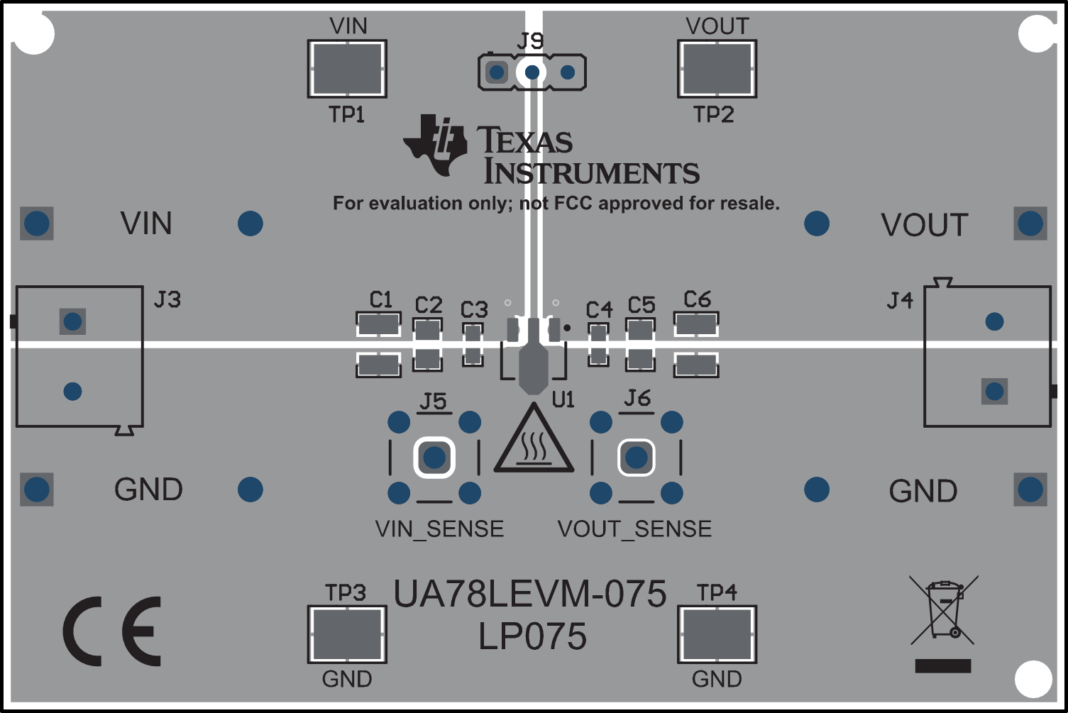
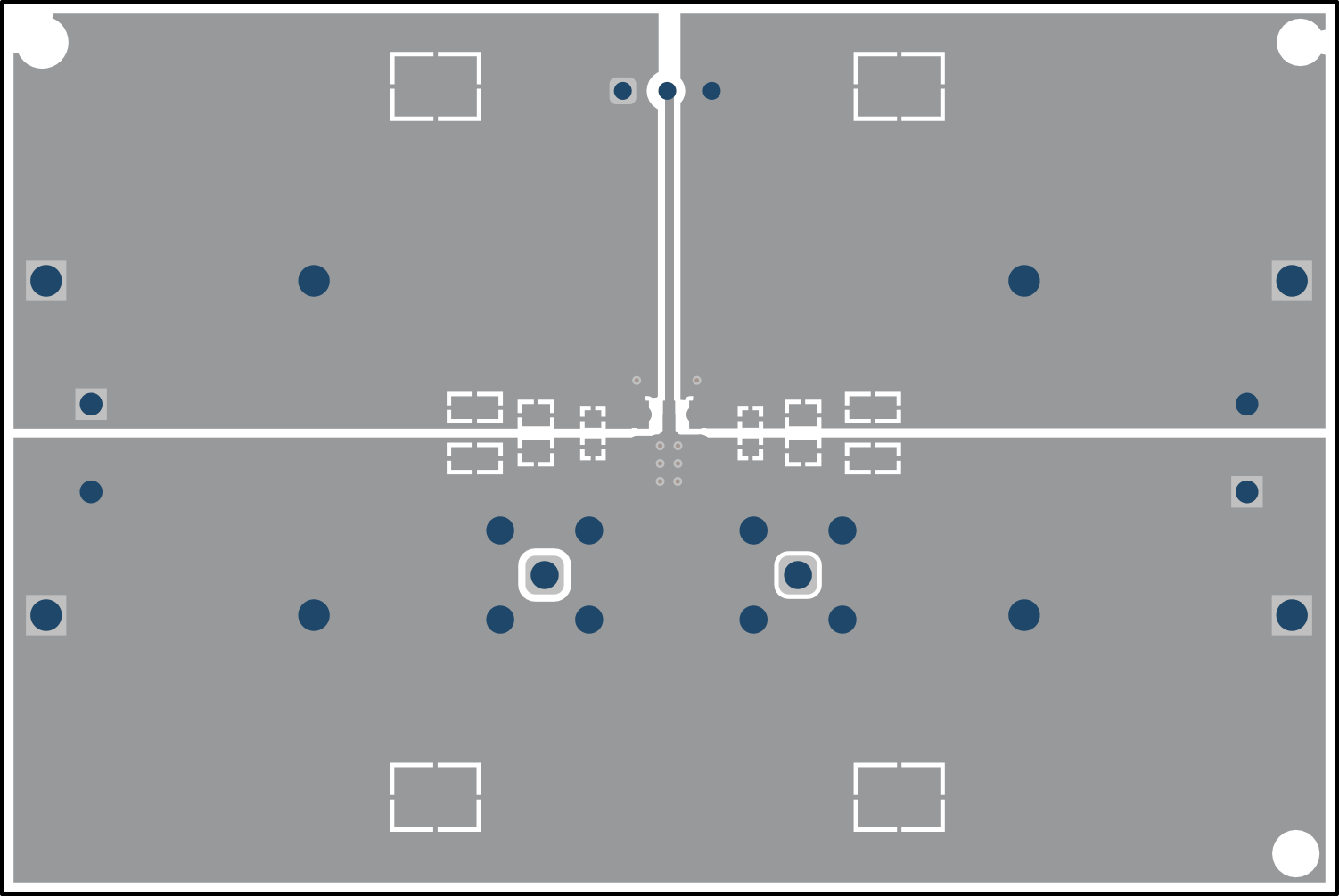
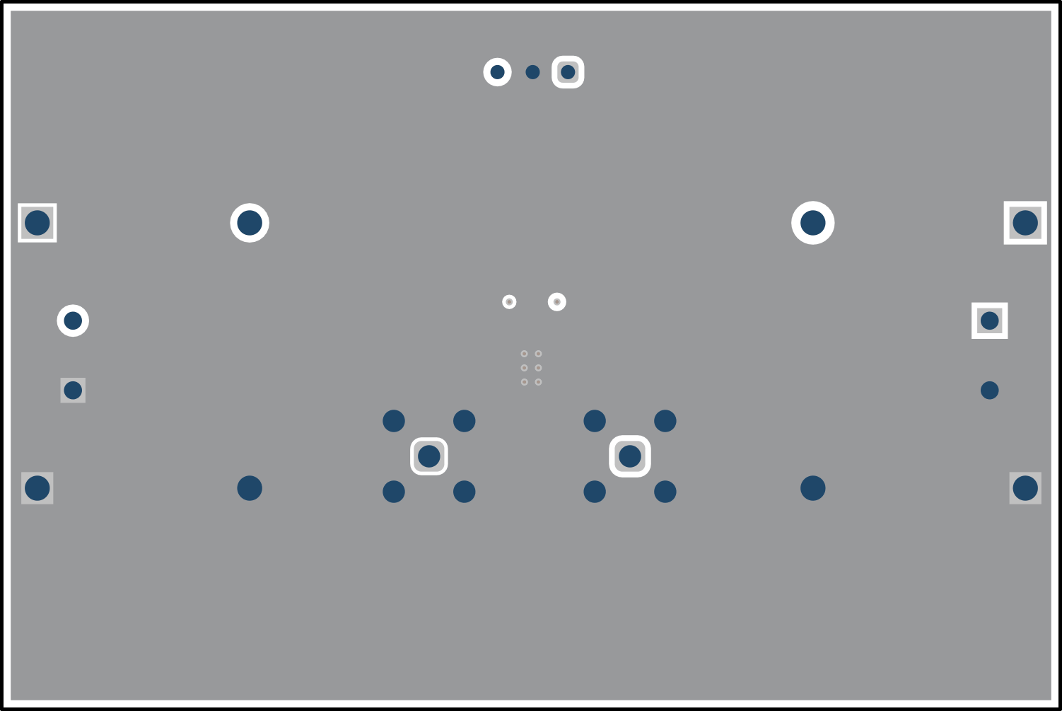
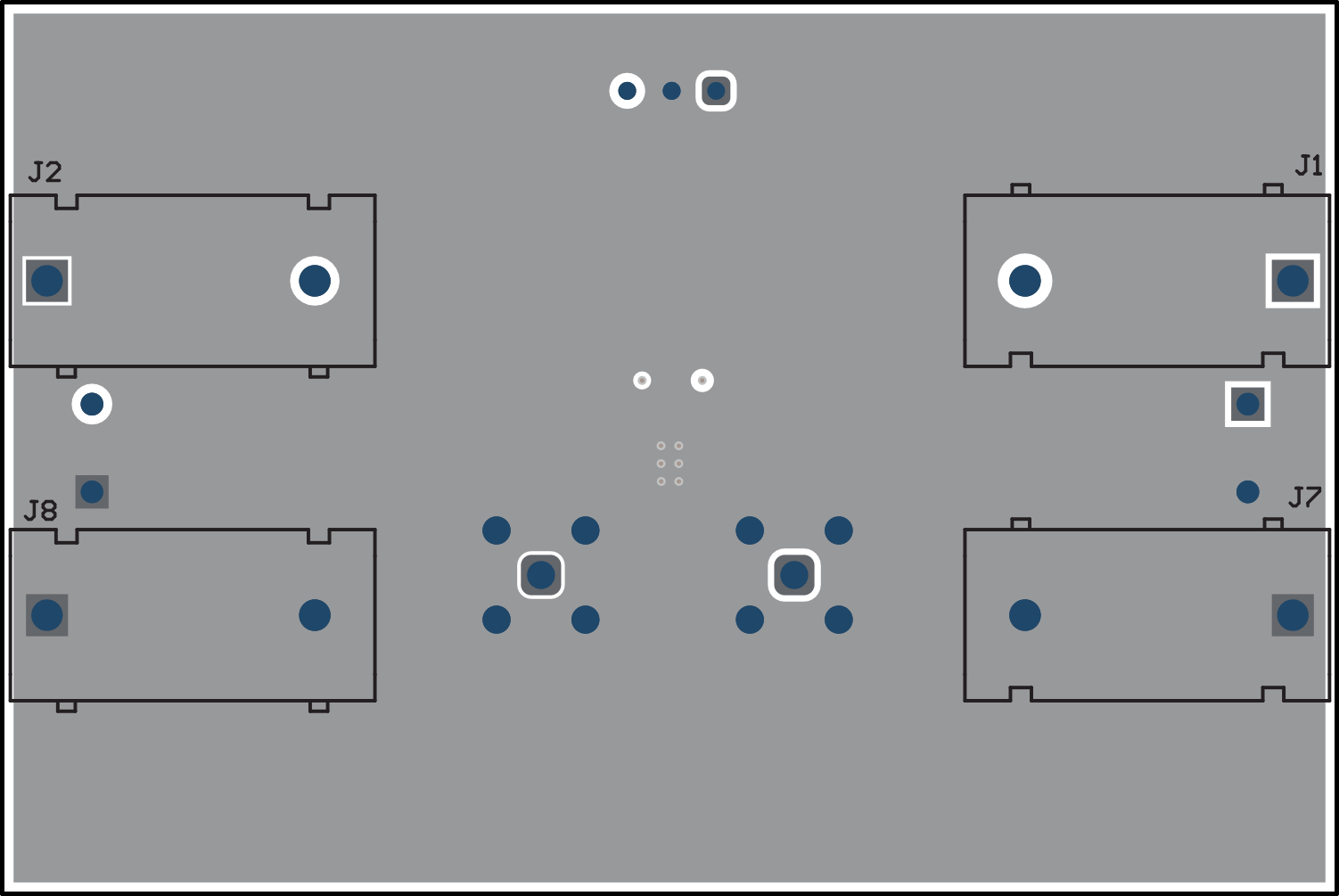
Figure 5-1 through Figure 5-4 illustrate the layout for the UA78LEVM-075.
 Figure 5-1 UA78LEVM-075 Top Assembly Layer and
Silkscreen
 Figure 5-2 UA78LEVM-075 Top Layer Routing
 Figure 5-3 UA78LEVM-075 Bottom Layer
Routing
 Figure 5-4 UA78LEVM-075 Bottom Assembly Layer and
Silkscreen