SLVU356A January 2010 – October 2021 TPS54290 , TPS54291
- Trademarks
- 1Introduction
- 2TPS54291EVM-431 Electrical Performance Specifications
-
3Schematic
- 3.1 Enable Jumpers (JP1 and JP2)
- 3.2 Error Amplifier Outputs
- 3.3
Test Point Descriptions
- 3.3.1 Input Voltage Monitoring (TP1 and TP2)
- 3.3.2 Channel 1 Output Voltage Monitoring (TP3 and TP4)
- 3.3.3 Channel 1 Loop Analysis (TP5, TP6, TP7, and TP8)
- 3.3.4 Channel 1 Switching Waveforms (TP9 and TP10)
- 3.3.5 TPS54291 IC Ground (TP11)
- 3.3.6 Channel 2 Switching Waveforms (TP12 and TP13)
- 3.3.7 Channel 2 Loop Analysis (TP14, TP15, TP16, and TP17)
- 3.3.8 Output Voltage Monitoring (TP18 and TP19)
- 4Test Setup
- 5TPS54291EVM-431 Typical Performance Data and Characteristic Curves
- 6EVM Assembly Drawings and Layout
- 7List of Materials
- 8Revision History
5.1 Efficiency

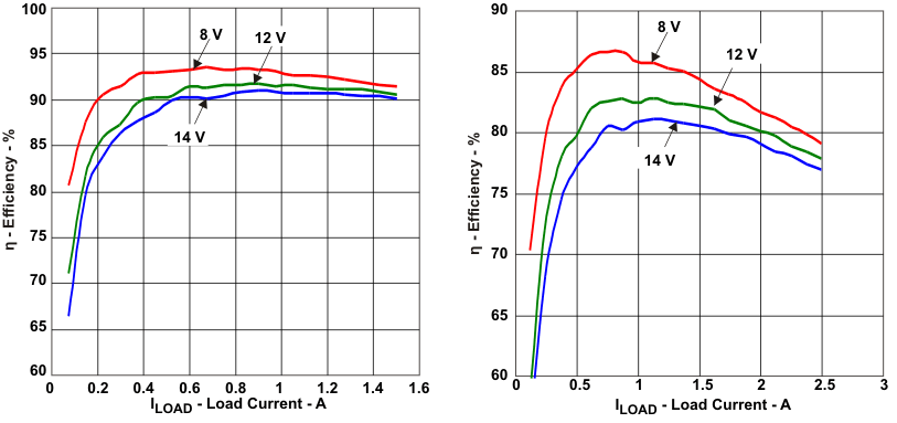
VIN = 9.6-13.2V, VOUT1 = 3.3V IOUT1 = 0-1.5A, VOUT2 = 1.2V IOUT2 = 0-2.5A
Figure 5-1 TPS54291EVM-431 Efficiency vs Load Current