SLVA528D September 2012 – August 2021 TPS65381-Q1 , TPS65381A-Q1
- Trademarks
- 1Introduction
- 2Product Overview
- 3Development Process for Management of Systematic Faults
- 4TPS65381x-Q1 Product Architecture for Management of Random Faults
-
5TPS65381x-Q1 Architecture Safety Mechanisms and Assumptions of Use
- 5.1 Power Supply
- 5.2 Regulated Supplies
- 5.3
Diagnostic, Monitoring, and Protection Functions
- 5.3.1 External MCU Fault Detection and Management
- 5.3.2 Voltage Monitor (VMON)
- 5.3.3 Loss-of-Clock Monitor (LCMON)
- 5.3.4 Junction Temperature Monitoring and Current Limiting
- 5.3.5 Analog and Digital MUX (AMUX and DMUX) and Diagnostic Output Pin (DIAG_OUT)
- 5.3.6 Analog Built-In Self-Test (ABIST)
- 5.3.7 Logic Built-In Self-Test (LBIST)
- 5.3.8 Device Configuration Register Protection
- 6Application Diagrams
- 7TPS65381x-Q1 as Safety Element out of Context (SEooC)
- 8Revision History
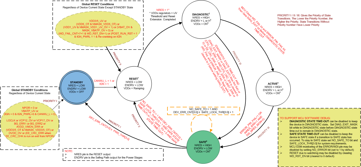
Device Operating States (continued)

(1) RESET State:
SPI, Watchdog and MCU ESM are in reset; see the data sheet for conditions that
prevent the wake up from the STANDBY state to the RESET state.
(2) DIAGNOSTIC
State: BIST (LBIST with ABIST) is initiated on the transition into the
DIAGNOSTIC state. See the data sheet for options to disable automatic BIST run,
the DIAGNOSTIC state time-out and diagnostics the MCU may perform on safety
functions. WD_FAIL_CNT reinitializes to 5 on transition into the DIAGNOSTIC
state.
(3) ACTIVE State:
WD_FAIL_CNT reinitializes to 5 during transition into the ACTIVE state. During
the ACTIVE state the MCU may perform diagnostics of some safety functions, see
the data sheet for more details.
(4) SAFE State:
DEV_ERR_CNT[3:0] increments on any transition to the SAFE state. See the data
sheet for details on SAFE state time-out.
(5) The ENDRV pin
level is dependent on the ENABLE_DRV bit, WD_FAIL_CNT[2:0] counter value, and
VDDx_OV as shown in Figure 4-2 in the DIAGNOSTIC and ACTIVE states.
(6) The VDD5 and
VSOUT1 regulators may be enabled or disabled in the DIAGNOSTIC, ACTIVE, and SAFE
states.
Figure 4-1 Device Controller State
Diagram