SLUSD37E October   2017  – November 2019

PRODUCTION DATA.  

  1. Features
  2. Applications
  3. Description
    1.     No Load Power
      1.      Device Images
        1.       Simplified Application
  4. Revision History
  5. Device Comparison Tables
  6. Pin Configuration and Functions
    1.     Pin Functions
  7. Specifications
    1. 7.1 Absolute Maximum Ratings
    2. 7.2 ESD Ratings
    3. 7.3 Recommended Operating Conditions
    4. 7.4 Thermal Information
    5. 7.5 Electrical Characteristics
    6. 7.6 Typical Characteristics
  8. Detailed Description
    1. 8.1 Overview
    2. 8.2 Functional Block Diagram
    3. 8.3 Feature Description
      1. 8.3.1 CrM/DCM Control Principle
      2. 8.3.2 Line Voltage Feed-Forward
        1. 8.3.2.1 Peak Line Voltage Detection
      3. 8.3.3 Valley Switching and CrM/DCM Hysteresis
        1. 8.3.3.1 Valley Delay Adjustment
      4. 8.3.4 Transconductance Amplifier with Transient Speed-up Function
      5. 8.3.5 Faults and Protections
        1. 8.3.5.1 Supply Undervoltage Lockout
        2. 8.3.5.2 Two Level Over-Current Protection
          1. 8.3.5.2.1 Cycle-by-Cycle Current Limit Ocp1
          2. 8.3.5.2.2 Ocp2 Gross Over-Current or CCM Protection
        3. 8.3.5.3 Output Over-Voltage Protection
          1. 8.3.5.3.1 First Level Output Over-Voltage Protection (Ovp1)
          2. 8.3.5.3.2 Second Level Over-Voltage Protection (Ovp2)
        4. 8.3.5.4 Thermal Shutdown Protection
        5. 8.3.5.5 Line Under-Voltage or Brown-In
      6. 8.3.6 High-Current Driver
    4. 8.4 Controller Functional Modes
      1. 8.4.1 Burst Mode Operation
      2. 8.4.2 Soft Start
  9. Application and Implementation
    1. 9.1 Application Information
    2. 9.2 Typical Application
      1. 9.2.1 Design Requirements
      2. 9.2.2 Detailed Design Procedure
        1. 9.2.2.1 Custom Design With WEBENCH® Tools
        2. 9.2.2.2 Power Stage Design
          1. 9.2.2.2.1 Boost Inductor Design
          2. 9.2.2.2.2 Boost Switch Selection
          3. 9.2.2.2.3 Boost Diode Selection
          4. 9.2.2.2.4 Output Capacitor Selection
        3. 9.2.2.3 ZCD/CS Pin
          1. 9.2.2.3.1 Voltage Spikes on the ZCD/CS pin Waveform
        4. 9.2.2.4 VOSNS Pin
        5. 9.2.2.5 Voltage Loop Compensation
          1. 9.2.2.5.1 Plant Model
          2. 9.2.2.5.2 Compensator Design
      3. 9.2.3 Application Curves
  10. 10Power Supply Recommendations
  11. 11Layout
    1. 11.1 Layout Guidelines
      1. 11.1.1 VOSNS Pin
      2. 11.1.2 ZCD/CS Pin
      3. 11.1.3 VCC Pin
      4. 11.1.4 GND Pin
      5. 11.1.5 DRV Pin
      6. 11.1.6 COMP Pin
    2. 11.2 Layout Example
  12. 12Device and Documentation Support
    1. 12.1 Custom Design With WEBENCH® Tools
    2. 12.2 Receiving Notification of Documentation Updates
    3. 12.3 Community Resources
    4. 12.4 Trademarks
    5. 12.5 Electrostatic Discharge Caution
    6. 12.6 Glossary
  13. 13Mechanical, Packaging, and Orderable Information

Burst Mode Operation

The UCC28056 controller provides leading light-load efficiency and standby power by implementing Burst mode of operation with the following key features:

  1. Power during burst is controlled to be approximately 11% of maximum output power for UCC28056/C and 16% of maximum power for UCC28056A/B for all Line voltage levels.
  2. During the Burst OFF period, the current consumption of UCC28056 drops to less than 132 μA.
  3. The TON pulse width is ramped up over the first four cycles, and ramped down over the last four cycles of each Burst-on period. This Soft-ON/OFF scheme ramps the Line current at the edge of each Burst ON period to limit audible noise and disturbance of the EMI filter.

Two comparator thresholds applied to the COMP pin voltage provide Burst Mode Operation. Switching halts after four soft-OFF cycles when the COMP pin voltage falls below the VBstFall threshold. Switching resumes with four Soft-ON cycles, when the COMP pin voltage rises above the VBstRise threshold. The average voltage of these two thresholds represents approximately 11% VCOMaxfor UCC28056/C and 16% VCOMax for UCC28056A/B. The power delivered during Burst ON is approximately 11% of maximum input power for UCC28056/C.
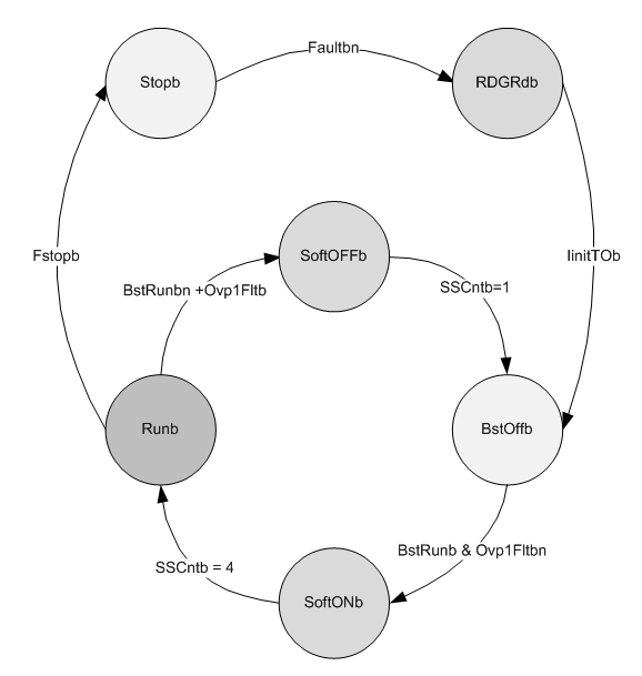
UCC28056 BstStateDia.gifFigure 25. Fault and Burst Mode State Diagram