SLUAA69 July 2020 – MONTH TPS548D22
6.2 Startup Waveforms and Behaviors Analysis Overview
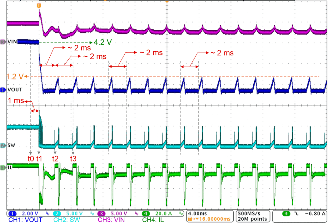
Figure 6-2 shows the start-up waveforms of TPS548D22 with 9.3-A load added before power up.
 Figure 6-2 Start-up
Waveforms with 9.3-A Load
Figure 6-2 Start-up
Waveforms with 9.3-A LoadAt t0, the device is enabled. t1 occurs after about 1 ms of the Power-on delay time, tPODLY. At t1, the device’s function modules, such as soft-start and protection functionality, start working. The soft-start begins from t1 for 1 ms with reference voltage ramping up from 0 V to the final defined level. The device does not start up because an OVP event also occurs at t1 and the output begins discharging to 0 V.
At t2, around 2 ms after t1, the output voltage begins ramping up to the OVP trip level of 1.2 V and then discharges to 0 V. At t3, the output voltage begins ramping up to the OVP level and discharges again, similar to at t2. The OVP event is periodically triggered every 2 ms. Hence, the device hiccups every 2 ms and gets stuck during the start-up state.
This may result in a number of questions. Why is the duration between t1 and t2 around 2 ms? Why does the device hiccup every 2 ms after t2? It is known that the hiccup time should be 16 ms for 1 ms soft-start. Here, a 2 ms hiccup time looks quite different. What about the behaviors of waveforms? How does the output ramp up and decay? Why does the software voltage ramp up following output and also have some pulses?
It can be seen from the inductor current and input voltage waveforms that when large inductor current transients occur, the input voltage changes sharply. This is not good for the input stage and should be avoided in the power supply design.
To address the questions listed above, the internal soft-start operation should be taken into account. Note that it is mentioned in Hiccup Mode and Latch-off Mode that when an OVP event occurs, the discharge of output could lead to an undervoltage condition and trigger the UVP. Then the OVP event will be reset by the UVP event. In addition, it is specified in UVP and OVP Functionality that UVP function is only enabled after the soft-start operation is completed.
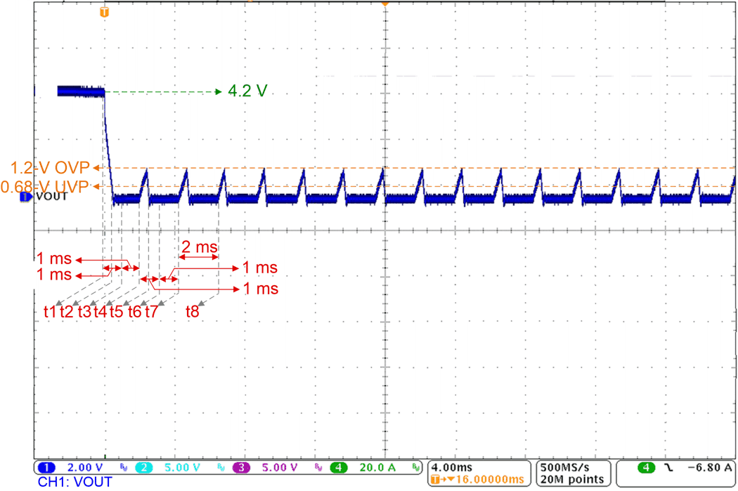
To better understand the relations between output behavior and internal soft-start operation. Figure 6-3 shows output voltage and critical time nodes in detail.
 Figure 6-3 Start-up
Output Waveforms with 9.3-A Load
Figure 6-3 Start-up
Output Waveforms with 9.3-A LoadThe OVP and UVP event occur cyclically. This results in a 2 ms hiccup time, consisting of 1 ms UVP delay and 1 ms soft-start time. If the circuit is configured with 2 ms soft-start time (by changing R24 to 47.5 kΩ), then the cycle is 3 ms hiccup time, consisting of 1 ms UVP delay and 2 ms soft-start time.