SBAU361 December 2020 ADC3664
2.1 ADC3664EVM Functionality
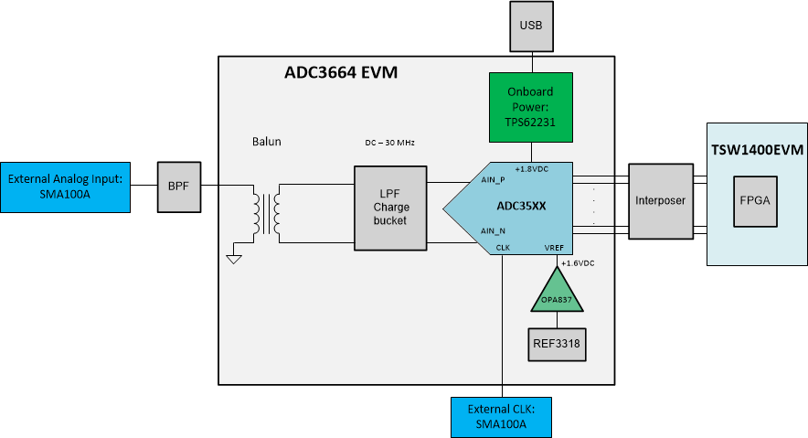
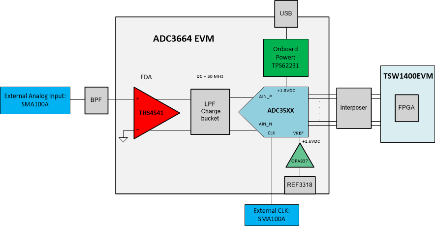
The ADC3664EVM receives power from the USB 2.0, +5 V rail, and is then converted to +3.3 VDC and +1.8 VDC. The ADC receives +1.8 VDC from the TPS62231 DC-DC converter. The power consumption of the 1.8 V rail can be monitored (using the INA226) in the ADC35xxEVM GUI. USB-to-SPI communication is established using the FTDI (FT4234H). The ADC clocks are supplied externally, and have limited functionality for the onboard CDCE6214 (Decimation modes only). The ADC3664 analog input can be AC coupled through the Balun (ADT1-6T+) input, or DC (or AC) coupled with the onboard FDA (THS4541). The analog input is 3.2 Vpp, and is driven a -1 dBFS (~2.8 Vpp) in all examples in this user's guide.
The ADC3664 has a +1.6 V voltage reference (VREF), and can be supplied internally or externally. By default, the EVM is configured to supply an external voltage reference using the REF3318 (divided down to +1.6V) and the OPA837 high speed amplifier to drive the voltage reference. At any time, the VREF can be changed to internal reference by SPI write.
The ADC3664 family uses an unbuffered analog input, so a glitch filter is required to attenuate the ADC sampling glitch from when the sampling capacitors switch (sample/hold). The glitch filter acts as a low pass filter with an corner frequency (Fc) at 30 MHz (accepts DC to 30 MHz). The Fc of the glitch filter can be modified by changing filter components.
The ADC3664EVM LVDS output data is routed to an FMC connector, and then connected to the LVDS Interposer card. This interposer card then maps to the TSW1400EVM's HSMC connector in order to capture the ADC36XXEVM SLVDS clock and data signals.
 Figure 2-1 ADC3664EVM Block Diagram: Balun Input
 Figure 2-2 ADC36xxEVM Block Diagram: FDA Input