SBAU361 December   2020 ADC3664


  1.   Trademarks
  2. 1Introduction
  3. 2Equipment
    1. 2.1 ADC3664EVM Functionality
    2. 2.2 Evaluation Board Feature Identification Summary
    3. 2.3 Required Equipment
  4. 3Setup Procedure
    1. 3.1 Install High-Speed Data Converter (HSDC) Pro Software
    2. 3.2 Install ADC35XXEVM GUI 1.0 Software
    3. 3.3 Connect the ADC3664 EVM and TSW1400EVM
    4. 3.4 Connect the Power Supply and Mini-USB Connections
    5. 3.5 Connect the Clocks and Analog Input
  5. 4Device Configuration
    1. 4.1 Bypass Mode
      1. 4.1.1 ADC35XX GUI: Bypass Mode Configuration
      2. 4.1.2 HSDC Pro: Bypass Mode
    2. 4.2 Real Decimation Mode
      1. 4.2.1 ADC35XX GUI: Real Decimation Mode Configuration
      2. 4.2.2 HSDC Pro: Real Decimation Mode
    3. 4.3 Complex Decimation Mode
      1. 4.3.1 ADC35XX GUI: Complex Decimation Configuration
      2. 4.3.2 HSDC PRO: Complex Decimation Mode
  6. 5Onboard FDA Configuration
  7. 6ADC3664EVM Power Monitor
  8. 7Test Pattern

Test Pattern

It is often useful to utilize test patterns to help verify the correct receipt of digital data at the microcontroller or FPGA. A ramp pattern can be enabled by following these steps:

  1. Click the yellow button "Analog Inputs and Clk".
  2. Next to "Test Pattern CHA", click the drop down menu, and select "RAMP CUSTOM". This can be done for "Test Pattern CHB" as well.
  3. In the field next to "Custom Pattern", enter the number "16".
  4. The digital ramp pattern is now enabled on the ADC. The output of the ADC is now a 14 bit, incrementing ramp pattern.
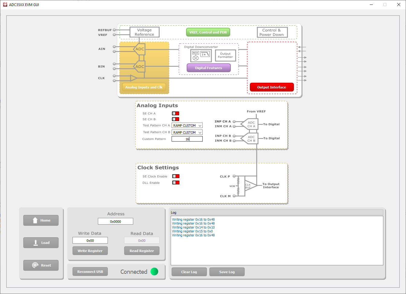
    GUID-0DBC20E5-7DDB-4339-A8D2-51CDDEC5DF3D-low.png Figure 7-1 ADC35XXEVM GUI 1.0 Ramp Pattern
  5. In HSDC Pro, the ramp pattern can now be seen when data is captured. These same steps apply to any data output mode (Bypass, Real Decimation and Complex Decimation).
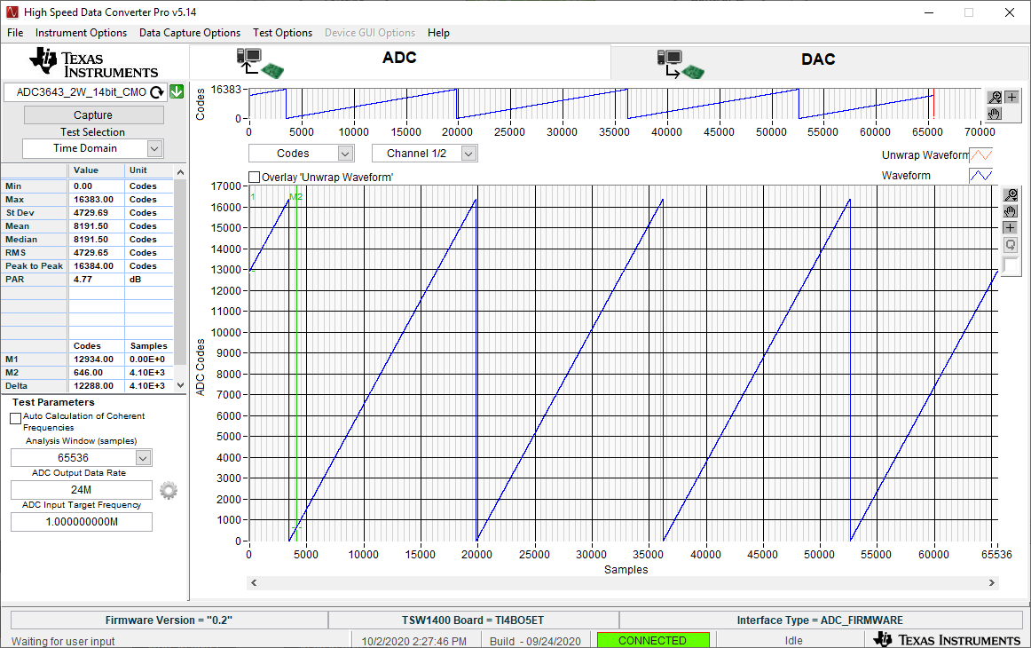
    GUID-01E14134-75FF-4821-9814-A2DE446BCA28-low.png Figure 7-2 HSDC Pro Digital Ramp Pattern