SBAU227A March   2014  – June 2021 TPS56520 , TPS56720 , TPS56920 , TPS56C20


  1.   Trademarks
  2. 1Introduction
  3. 2Performance Specification Summary
  4. 3Modifications
    1. 3.1 Output Voltage Set Point
    2. 3.2 Output Voltage Set Point Using I2C Interface
      1. 3.2.1 PC Preparation
      2. 3.2.2 Connect the PC
      3. 3.2.3 Voltage Scaling Procedure
    3. 3.3 Output Filter and Closed Loop Response
  5. 4Test Setup and Results
    1. 4.1 Input/Output Connections
    2. 4.2 Start Up Procedure
    3. 4.3 Efficiency
    4. 4.4 Load Regulation
    5. 4.5 Line Regulation
    6. 4.6 Load Transient Response
    7. 4.7 Output Voltage Ripple
    8. 4.8 Start Up
    9. 4.9 Shut Down
  6. 5Board Layout
    1. 5.1 Board Layout
  7. 6Schematic, Bill of Materials and Reference
    1. 6.1 Schematic
    2. 6.2 Bill of Materials
    3. 6.3 Reference
  8. 7Revision History

Load Transient Response

Figure 4-5 shows the TPS56C20EVM-614 response to load transient. The current step is from 50 mA to 12 A (0% to 100% of rated load), with a slew rate of 500 mA/µs. Figure 4-5 shows the total peak-to-peak output voltage variation.
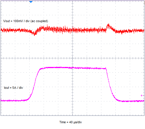
GUID-11D6BE42-76F1-425C-8678-AAF498525716-low.pngFigure 4-5 TPS56C20EVM-614 Load Transient Response