SBAS895B May 2018 – April 2020
PRODUCTION DATA.
- 1 Features
- 2 Applications
- 3 Description
- 4 Revision History
- 5 Device Comparison Table
- 6 Pin Configuration and Functions
-
7 Specifications
- 7.1 Absolute Maximum Ratings
- 7.2 ESD Ratings
- 7.3 Recommended Operating Conditions
- 7.4 Thermal Information
- 7.5 Power Ratings
- 7.6 Insulation Specifications
- 7.7 Safety-Related Certifications
- 7.8 Safety Limiting Values
- 7.9 Electrical Characteristics
- 7.10 Switching Characteristics
- 7.11 Insulation Characteristics Curves
- 7.12 Typical Characteristics
- 8 Detailed Description
- 9 Application and Implementation
- 10Power Supply Recommendations
- 11Layout
- 12Device and Documentation Support
- 13Mechanical, Packaging, and Orderable Information
8.3.3 Fail-Safe Output
The AMC1300 offers a fail-safe output that simplifies diagnostics on a system level. The fail-safe output is active in two cases:
- When the high-side supply VDD1 of the AMC1300 is missing, or
- When the common-mode input voltage, that is VCM = (VINP + VINN) / 2, exceeds the minimum common-mode overvoltage detection level VCMov of VDD1 – 2 V.
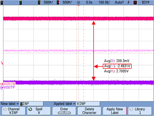
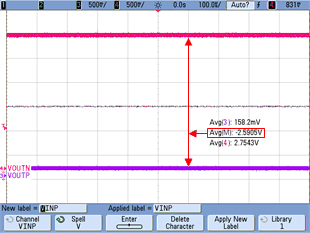
Figure 49 and Figure 50 show the fail-safe output of the AMC1300 as a negative differential output voltage value that does not occur under normal device operation. Use the VFAILSAFE voltage specified in the Electrical Characteristics table as a reference value for the fail-safe detection on a system level.
 Figure 49. Typical Negative Clipping Output of the AMC1300
  Figure 50. Typical Fail-Safe Output of the AMC1300