ZHCSAY5D march   2013  – april 2021 UCD3138064

PRODUCTION DATA  

  1. 特性
  2. 应用
  3. 说明
  4. Functional Block Diagram
  5. Revision History
  6. Device Options
    1. 6.1 Device Comparison Table
    2. 6.2 Product Selection Matrix
  7. Pin Configuration and Functions
    1. 7.1 Pin Diagrams
    2. 7.2 Pin Functions
  8. Specifications
    1. 8.1  Absolute Maximum Ratings #GUID-DB56AA00-A5E9-4426-9853-ACC9CCD10656/SLUSB727999
    2. 8.2  Handling Ratings
    3. 8.3  Recommended Operating Conditions
    4. 8.4  Thermal Information
    5. 8.5  Electrical Characteristics
    6. 8.6  Timing Characteristics
    7. 8.7  PMBus/SMBus/I2C Timing
    8. 8.8  Power On Reset (POR) / Brown Out Reset (BOR)
    9. 8.9  Typical Clock Gating Power Savings
    10. 8.10 Typical Characteristics
  9. Detailed Description
    1. 9.1 Overview
      1. 9.1.1 ARM Processor
      2. 9.1.2 Memory
    2. 9.2 Functional Block Diagram
    3. 9.3 Feature Description
      1. 9.3.1  System Module
        1. 9.3.1.1 Address Decoder (DEC)
        2. 9.3.1.2 Memory Management Controller (MMC)
        3. 9.3.1.3 System Management (SYS)
        4. 9.3.1.4 Central Interrupt Module (CIM)
      2. 9.3.2  Peripherals
        1. 9.3.2.1 Digital Power Peripherals
          1. 9.3.2.1.1 Front End
          2. 9.3.2.1.2 DPWM Module
          3. 9.3.2.1.3 DPWM Events
          4. 9.3.2.1.4 High Resolution DPWM
          5. 9.3.2.1.5 Over Sampling
          6. 9.3.2.1.6 DPWM Interrupt Generation
          7. 9.3.2.1.7 DPWM Interrupt Scaling/Range
      3. 9.3.3  Automatic Mode Switching
        1. 9.3.3.1 Phase Shifted Full Bridge Example
        2. 9.3.3.2 LLC Example
        3. 9.3.3.3 Mechanism For Automatic Mode Switching
      4. 9.3.4  DPWMC, Edge Generation, Intramux
      5. 9.3.5  Filter
        1. 9.3.5.1 Loop Multiplexer
        2. 9.3.5.2 Fault Multiplexer
      6. 9.3.6  Communication Ports
        1. 9.3.6.1 SCI (UART) Serial Communication Interface
        2. 9.3.6.2 PMBUS/I2C
        3. 9.3.6.3 SPI
      7. 9.3.7  Real Time Clock
      8. 9.3.8  Timers
        1. 9.3.8.1 24-Bit Timer
        2. 9.3.8.2 16-Bit PWM Timers
        3. 9.3.8.3 Watchdog Timer
      9. 9.3.9  General Purpose ADC12
      10. 9.3.10 Miscellaneous Analog
      11. 9.3.11 Brownout
      12. 9.3.12 Global I/O
      13. 9.3.13 Temperature Sensor Control
      14. 9.3.14 I/O Mux Control
      15. 9.3.15 Current Sharing Control
      16. 9.3.16 Temperature Reference
    4. 9.4 Device Functional Modes
      1. 9.4.1 DPWM Modes Of Operation
        1. 9.4.1.1 Normal Mode
        2. 9.4.1.2 Phase Shifting
        3. 9.4.1.3 DPWM Multiple Output Mode
        4. 9.4.1.4 DPWM Resonant Mode
      2. 9.4.2 Triangular Mode
      3. 9.4.3 Leading Edge Mode
    5. 9.5 Memory
      1. 9.5.1 Register Maps
        1. 9.5.1.1 CPU Memory Map and Interrupts
          1. 9.5.1.1.1 Memory Map (After Reset Operation)
          2. 9.5.1.1.2 Memory Map (Normal Operation)
          3. 9.5.1.1.3 Memory Map (System and Peripherals Blocks)
        2. 9.5.1.2 Boot ROM
        3. 9.5.1.3 Customer Boot Program
        4. 9.5.1.4 Flash Management
        5. 9.5.1.5 Synchronous Rectifier MOSFET Ramp and IDE Calculation
  10. 10Applications and Implementation
    1. 10.1 Application Information
    2. 10.2 Typical Application
      1. 10.2.1 Design Requirements
      2. 10.2.2 Detailed Design Procedure
        1. 10.2.2.1 PCMC (Peak Current Mode Control) PSFB (Phase Shifted Full Bridge) Hardware Configuration Overview
        2. 10.2.2.2 DPWM Initialization for PSFB
          1. 10.2.2.2.1 DPWM Synchronization
        3. 10.2.2.3 Fixed Signals to Bridge
        4. 10.2.2.4 Dynamic Signals to Bridge
        5. 10.2.2.5 System Initialization for PCM
          1. 10.2.2.5.1 Use of Front Ends and Filters in PSFB
          2. 10.2.2.5.2 Peak Current Detection
          3. 10.2.2.5.3 Peak Current Mode (PCM)
      3. 10.2.3 Application Curves
  11. 11Power Supply Recommendations
    1. 11.1 Introduction To Power Supply and Layout Recommendations
    2. 11.2 3.3-V Supply Pins
    3. 11.3 Recommendation for V33 Ramp up Slew Rate for UCD3138 and UCD3138064
    4. 11.4 Recommendation for RC Time Constant of RESET Pin for UCD3138 and UCD3138064
  12. 12Layout
    1. 12.1 Layout Guidelines
      1. 12.1.1 EMI and EMC Mitigation Guidelines
      2. 12.1.2 BP18 Pin
      3. 12.1.3 Additional Bias Guidelines
      4.      UCD3138 Pin Connection Recommendation
        1. 12.1.4.1 Current Amplifier With EADC Connection
        2. 12.1.4.2 DPWM Synchronization
        3. 12.1.4.3 External Clock
        4. 12.1.4.4 GPIOS
        5. 12.1.4.5 DPWM PINS
        6. 12.1.4.6 EAP and EAN Pins
        7. 12.1.4.7 ADC Pins
          1. 12.1.4.7.1 RESET Pin
      5. 12.1.4 UART Communication Port
      6.      Special Considerations
    2. 12.2 Layout Example
      1. 12.2.1 UCD3138 and UCD3138064 40 Pin
      2. 12.2.2 UCD3138 and UCD3138064 64 Pin
  13. 13Device and Documentation Support
    1. 13.1 Device Support
    2. 13.2 Documentation Support
      1. 13.2.1 Related Documentation
    3. 13.3 Trademarks
    4. 13.4 静电放电警告
    5. 13.5 术语表
  14. 14Mechanical, Packaging, and Orderable Information

封装选项

机械数据 (封装 | 引脚)
散热焊盘机械数据 (封装 | 引脚)
订购信息

Normal Mode

In Normal mode, the Filter output determines the pulse width on DPWM A. DPWM B fits into the rest of the switching period, with a dead time separating it from the DPWM A on-time. It is useful for buck topologies, among others. Here is a drawing of the Normal Mode waveforms:
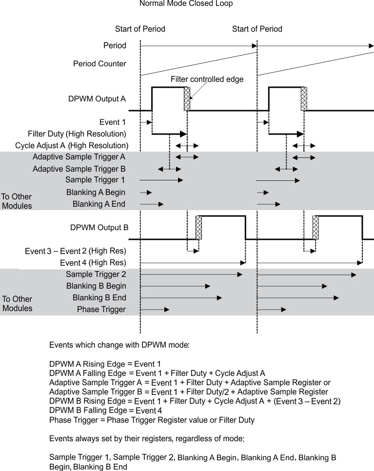
GUID-A5E82984-DEE8-43E5-A81E-7D215BCA4350-low.gifFigure 9-22 Normal Mode - Closed Loop

Cycle adjust A can be used to adjust pulse widths on individual phases of a multi-phase system. This can be used for functions like current balancing. The Adaptive Sample Triggers can be used to sample in the middle of the on-time (for an average output), or at the end of the on-time (to minimize phase delay) The Adaptive Sample Register provides an offset from the center of the on-time. This can compensate for external delays, such as MOSFET and gate driver turn on times.

Blanking A-Begin and Blanking A-End can be used to blank out noise from the MOSFET turn on at the beginning of the period (DPWMA rising edge). Blanking B could be used at the turn off time of DPWMB. The other edges are dynamic, so blanking is more difficult.

Cycle Adjust B has no effect in Normal Mode.