ZHCSAY5D march 2013 – april 2021 UCD3138064
PRODUCTION DATA
- 1 特性
- 2 应用
- 3 说明
- 4 Functional Block Diagram
- 5 Revision History
- 6 Device Options
- 7 Pin Configuration and Functions
-
8 Specifications
- 8.1 Absolute Maximum Ratings #GUID-DB56AA00-A5E9-4426-9853-ACC9CCD10656/SLUSB727999
- 8.2 Handling Ratings
- 8.3 Recommended Operating Conditions
- 8.4 Thermal Information
- 8.5 Electrical Characteristics
- 8.6 Timing Characteristics
- 8.7 PMBus/SMBus/I2C Timing
- 8.8 Power On Reset (POR) / Brown Out Reset (BOR)
- 8.9 Typical Clock Gating Power Savings
- 8.10 Typical Characteristics
-
9 Detailed Description
- 9.1 Overview
- 9.2 Functional Block Diagram
- 9.3
Feature Description
- 9.3.1 System Module
- 9.3.2 Peripherals
- 9.3.3 Automatic Mode Switching
- 9.3.4 DPWMC, Edge Generation, Intramux
- 9.3.5 Filter
- 9.3.6 Communication Ports
- 9.3.7 Real Time Clock
- 9.3.8 Timers
- 9.3.9 General Purpose ADC12
- 9.3.10 Miscellaneous Analog
- 9.3.11 Brownout
- 9.3.12 Global I/O
- 9.3.13 Temperature Sensor Control
- 9.3.14 I/O Mux Control
- 9.3.15 Current Sharing Control
- 9.3.16 Temperature Reference
- 9.4 Device Functional Modes
- 9.5 Memory
-
10Applications and
Implementation
- 10.1 Application Information
- 10.2
Typical Application
- 10.2.1 Design Requirements
- 10.2.2 Detailed Design Procedure
- 10.2.3 Application Curves
- 11Power Supply Recommendations
- 12Layout
- 13Device and Documentation Support
- 14Mechanical, Packaging, and Orderable Information
封装选项
机械数据 (封装 | 引脚)
散热焊盘机械数据 (封装 | 引脚)
订购信息
10.2.2.4 Dynamic Signals to Bridge
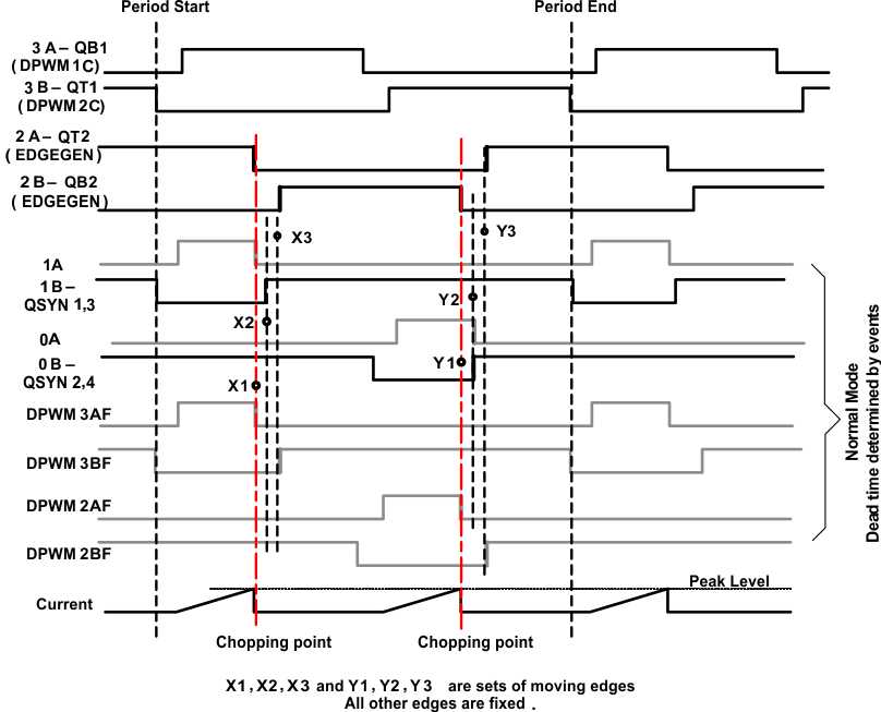
DPWM0 and 1 are set at normal mode. PCMC triggering signal (fault) chops DPWM0A and 1A cycle by cycle. The corresponding DPWM0B and 1B are used for synchronous rectifier MOSFET control. The same PCMC triggering signal is applied to DPWM2 and DPWM3. Both of these are set to normal mode as well. DPWM2 and 3 are chopped and their edges are used to generate the next two dynamic signals to the bridge. They are generated using the Edge Generator Module in DPWM2. The Edge Generator sources are DPWM2 and DPWM3. The edges used are:
| DPWM2A turned on by a rising edge on DPWM2BF DPWM2A turned off by a falling edge on DPWM3AF DPWM2B turned on by a rising edge on DPWM3BF DPWM2B turned off by a falling edge on DPWM2AF |
 Figure 10-6 Dynamic Signals to Bridge
The Edge Generator is configured with these statements:
| Dpwm2Regs.DPWMEDGEGEN.bit.A_ON_EDGE = 2; Dpwm2Regs.DPWMEDGEGEN.bit.A_OFF_EDGE = 5; Dpwm2Regs.DPWMEDGEGEN.bit.B_ON_EDGE = 6; Dpwm2Regs.DPWMEDGEGEN.bit.B_OFF_EDGE = 1; | |
| Dpwm2Regs.DPWMCTRL0.bit.PWM_A_INTRA_MUX = 1; // EDGEGEN-A out the A output Dpwm2Regs.DPWMCTRL0.bit.PWM_B_INTRA_MUX = 1; // EDGEGEN-B out the B output | |
| Dpwm2Regs.DPWMEDGEGEN.bit.EDGE_EN = 1; |
The EDGE_EN bits are set for all 4 DPWMs. This is done to ensure that all signals have the same timing delay through the DPWM.
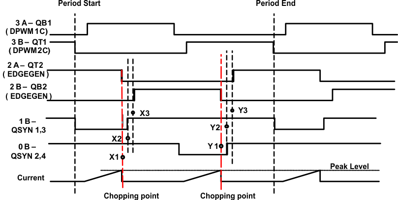
The finial 6 gate signals are shown in Figure 10-7.
 Figure 10-7 Final 6 Gate Signals
Note how the falling edge of DPWM2AF aligns with the X1 edge, and how the rising edge of DPWM2BF aligns with the X3 edge. The falling edges on DPWM2AF and DPWM3AF are caused by the peak detection logic. This is fed through the Cycle By Cycle logic. The Cycle By Cycle logic also has a special feature to control the rising edges of DPWM2BF (X1 and X3) and DPWM3BF (Y1 and Y3). It uses the value of Event3 – Event2 to control the time between the edges. The same feature is used with DPWM0 and DPWM1 to control the X2 and Y2 signals. Using the other 2 DPWMs permits these signals to have a different dead time.
The same setup can be used for voltage mode control. In this case, the Filter output sets the timing of the falling edge on DPWMxAF.
All DPWMs are configured in Normal mode, with CBC enabled. If external slope compensation is used, DPWM1A and DPWM1B are used to reset the external compensator at the beginning of each half cycle. If no PCMC event occurs, the values of Events 2 and 3 determine the locations of the edges, just as in open loop mode.