SLUSA16D March 2010 – November 2016 UCC28950
PRODUCTION DATA.
- 1 Features
- 2 Applications
- 3 Description
- 4 Revision History
- 5 Pin Configuration and Functions
- 6 Specifications
-
7 Detailed Description
- 7.1 Overview
- 7.2 Functional Block Diagram
- 7.3
Feature Description
- 7.3.1 Start-Up Protection Logic
- 7.3.2 Voltage Reference (VREF)
- 7.3.3 Error Amplifier (EA+, EA-, COMP)
- 7.3.4 Soft Start and Enable (SS/EN)
- 7.3.5 Light-Load Power Saving Features
- 7.3.6 Adaptive Delay, (Delay between OUTA and OUTB, OUTC and OUTD (DELAB, DELCD, ADEL))
- 7.3.7 Adaptive Delay (Delay between OUTA and OUTF, OUTB and OUTE (DELEF, ADELEF))
- 7.3.8 Minimum Pulse (TMIN)
- 7.3.9 Burst Mode
- 7.3.10 Switching Frequency Setting
- 7.3.11 Slope Compensation (RSUM)
- 7.3.12 Dynamic SR ON/OFF Control (DCM Mode)
- 7.3.13 Current Sensing (CS)
- 7.3.14 Cycle-by-Cycle Current Limit Current Protection and Hiccup Mode
- 7.3.15 Synchronization (SYNC)
- 7.3.16 Outputs (OUTA, OUTB, OUTC, OUTD, OUTE, OUTF)
- 7.3.17 Supply Voltage (VDD)
- 7.3.18 Ground (GND)
- 7.4 Device Functional Modes
-
8 Application and Implementation
- 8.1 Application Information
- 8.2
Typical Application
- 8.2.1 Design Requirements
- 8.2.2
Detailed Design Procedure
- 8.2.2.1 Power Loss Budget
- 8.2.2.2 Preliminary Transformer Calculations (T1)
- 8.2.2.3 QA, QB, QC, QD FET Selection
- 8.2.2.4 Selecting LS
- 8.2.2.5 Selecting Diodes DB and DC
- 8.2.2.6 Output Inductor Selection (LOUT)
- 8.2.2.7 Output Capacitance (COUT)
- 8.2.2.8 Select FETs QE and QF
- 8.2.2.9 Input Capacitance (CIN)
- 8.2.2.10 Current Sense Network (CT, RCS, R7, DA)
- 8.2.3 Application Curves
- 9 Power Supply Recommendations
- 10Layout
- 11Device and Documentation Support
- 12Mechanical, Packaging, and Orderable Information
6 Specifications
6.1 Absolute Maximum Ratings
over operating free-air temperature range (unless otherwise noted) (1)(2)| MIN | MAX | UNIT | ||
|---|---|---|---|---|
| Input supply voltage, VDD (3) | –0.4 | 20 | V | |
| OUTA, OUTB, OUTC, OUTD, OUTE, OUTF | –0.4 | VDD + 0.4 | V | |
| Input voltage on DELAB, DELCD, DELEF, SS/EN, DCM, TMIN, RT, SYNC, RSUM, EA+, EA-, COMP, CS, ADEL, ADELEF | –0.4 | VREF + 0.4 | V | |
| Output voltage on VREF | –0.4 | 5.6 | V | |
| Continuous total power dissipation | See Dissipation Ratings | |||
| Operating virtual junction temperature, TJ | –40 | +150 | °C | |
| Operating ambient temperature, TA | –40 | +125 | °C | |
| Lead temperature (soldering, 10 sec.) | +300 | °C | ||
| Storage temperature, Tstg | –65 | +150 | °C | |
(1) Stresses beyond those listed under Absolute Maximum Ratings may cause permanent damage to the device. These are stress ratings only, and functional operation of the device at these or any other conditions beyond those indicated under Recommended Operating Conditions is not implied. Exposure to absolute-maximum-rated conditions for extended periods may affect device reliability.
(2) These devices are sensitive to electrostatic discharge; follow proper device handling procedures.
(3) All voltages are with respect to GND unless otherwise noted. Currents are positive into, negative out of the specified terminal. See Packaging Section of the datasheet for thermal limitations and considerations of packages.
6.2 ESD Ratings
| VALUE | UNIT | |||
|---|---|---|---|---|
| V(ESD) | Electrostatic discharge | Human body model (HBM), per ANSI/ESDA/JEDEC JS-001(1) | 2000 | V |
| Charged device model (CDM), per JEDEC specification JESD22-C101(2) | 500 | V | ||
(1) JEDEC document JEP155 states that 500-V HBM allows safe manufacturing with a standard ESD control process.
(2) JEDEC document JEP157 states that 250-V CDM allows safe manufacturing with a standard ESD control process.
6.3 Recommended Operating Conditions
over operating free-air temperature range (unless otherwise noted)| MIN | NOM | MAX | UNIT | |
|---|---|---|---|---|
| Supply voltage range, VDD | 8 | 12 | 17 | V |
| Operating junction temperature range | –40 | 125 | °C | |
| Converter switching frequency setting range, FSW(nom) | 50 | 1000 | kHz | |
| Programmable delay range between OUTA, OUTB and OUTC, OUTD set by resistors DELAB and DELCD and parameter KA(1) | 30 | 1000 | ns | |
| Programmable delay range between OUTA, OUTF and OUTB, OUTE set by resistor DELEF, and parameter KEF(1) | 30 | 1400 | ns | |
| Programmable DCM range as percentage of voltage at CS(1) | 5% | 30% | ||
| Programmable TMIN range | 100 | 800 | ns |
(1) Verified during characterization only.
6.4 Thermal Information
| THERMAL METRIC(1) | UCC28950 | UNIT | |
|---|---|---|---|
| PW (TSSOP) | |||
| 24 PINS | |||
| RθJA | Junction-to-ambient thermal resistance | 93.3 | °C/W |
| RθJC(top) | Junction-to-case (top) thermal resistance | 24.2 | °C/W |
| RθJB | Junction-to-board thermal resistance | 47.9 | °C/W |
| ψJT | Junction-to-top characterization parameter | 0.7 | °C/W |
| ψJB | Junction-to-board characterization parameter | 47.4 | °C/W |
| RθJC(bot) | Junction-to-case (bottom) thermal resistance | n/a | °C/W |
(1) For more information about traditional and new thermal metrics, see the Semiconductor and IC Package Thermal Metrics application report, SPRA953.
6.5 Electrical Characteristics
VDD = 12 V, TA = TJ = –40°C to +125°C, CVDD = 1 µF, CREF = 1 µF, RAB = 22.6 kΩ, RCD = 22.6 kΩ , REF = 13.3 kΩ, RSUM = 124 kΩ, RTMIN = 88.7 kΩ, RT = 59 kΩ connected between RT pin and 5-V voltage supply to set FSW = 100 kHz (FOSC = 200 kHz) (unless otherwise noted). All component designations are from Figure 48.| PARAMETER | TEST CONDITIONS | MIN | TYP(1) | MAX | UNIT | |
|---|---|---|---|---|---|---|
| UNDERVOLTAGE LOCKOUT (UVLO) | ||||||
| UVLO_RTH | Start threshold | 6.75 | 7.3 | 7.9 | V | |
| UVLO_FTH | Minimum operating voltage after start | 6.15 | 6.7 | 7.2 | V | |
| UVLO_HYST | Hysteresis | 0.53 | 0.6 | 0.75 | V | |
| SUPPLY CURRENTS | ||||||
| IDD(off) | Startup current | VDD is 5.2 V | 150 | 270 | µA | |
| IDD | Operating supply current | 5 | 10 | mA | ||
| VREF OUTPUT VOLTAGE | ||||||
| VREF | VREF total output range | 0 ≤ IR ≤ 20 mA; VDD = from 8 V to 17 V | 4.925 | 5 | 5.075 | V |
| ISCC | Short circuit current | VREF = 0 V | –53 | –23 | mA | |
| SWITCHING FREQUENCY (½ OF INTERNAL OSCILLATOR FREQUENCY FOSC) | ||||||
| FSW(nom) | Total range | 92 | 100 | 108 | kHz | |
| DMAX | Maximum duty cycle | 95% | 97% | |||
| SYNCHRONIZATION | ||||||
| PHSYNC | Total range | RT = 59 kΩ between RT and GND; Input pulses 200 kHz, D = 0.5 at SYNC | 85 | 90 | 95 | °PH |
| FSYNC | Total range | RT = 59 kΩ between RT and 5 V; –40 °C ≤ TJ ≤ +125°C | 180 | 200 | 220 | kHz |
| TPW | Pulse width | 2.2 | 2.5 | 2.8 | µs | |
| ERROR AMPLIFIER | ||||||
| VICM | Common mode input voltage range | VICM range ensures parameters, the functionality ensured for 3.6 V < VICM < VREF + 0.4 V, and –0.4 V < VICM < 0.5 V | 0.5 | 3.6 | V | |
| VIO | Offset voltage | – 7 | 7 | mV | ||
| IBIAS | Input bias current | –1 | 1 | µA | ||
| EAHIGH | High-level output voltage | (EA+) – (EA–) = 500 mV, IEAOUT = –0.5 mA | 3.9 | 4.25 | V | |
| EALOW | Low-level output voltage | (EA+) – (EA–) = –500 mV, IEAOUT = 0.5 mA | 0.25 | 0.35 | V | |
| ISOURCE | Error amplifier source current | –8 | –3.75 | –0.5 | mA | |
| ISINK | Error amplifier sink current | 2.7 | 4.6 | 5.75 | mA | |
| IVOL | Open-loop dc gain | 100 | dB | |||
| GBW | Unity gain bandwidth(1) | 3 | MHz | |||
| CYCLE-BY-CYCLE CURRENT LIMIT | ||||||
| VCS_LIM | CS pin cycle-by-cycle threshold | 1.94 | 2 | 2.06 | V | |
| INTERNAL HICCUP MODE SETTINGS | ||||||
| IDS | Discharge current to set cycle-by-cycle current limit duration | CS = 2.5 V, VSS = 4 V | 15 | 20 | 25 | µA |
| VHCC | Hiccup OFF Time threshold | 3.2 | 3.6 | 4.2 | V | |
| IHCC | Discharge current to set Hiccup Mode OFF Time | 1.90 | 2.55 | 3.2 | µA | |
| SOFT START/ENABLE | ||||||
| ISS | Charge current | VSS = 0 V | 20 | 25 | 30 | µA |
| VSS_STD | Shutdown/restart/reset threshold | 0.25 | 0.50 | 0.70 | V | |
| VSS_PU | Pull up threshold | 3.3 | 3.7 | 4.3 | V | |
| VSS_CL | Clamp voltage | 4.20 | 4.65 | 4.95 | V | |
| LIGHT-LOAD EFFICIENCY CIRCUIT | ||||||
| VDCM | DCM threshold, T = 25°C | VDCM = 0.4 V, Sweep CS confirm there are OUTE and OUTF pulses | 0.37 | 0.39 | 0.41 | V |
| DCM threshold, T = 0°C to +85°C (7) | VDCM = 0.4 V, Sweep CS, confirm there are OUTE and OUTF pulses | 0.364 | 0.390 | 0.416 | V | |
| DCM threshold, T= –40°C to +125°C (7) | VDCM = 0.4 V, Sweep CS, confirm there are OUTE and OUTF pulses | 0.35 | 0.39 | 0.43 | V | |
| IDCM_SRC | DCM Sourcing Current | CS < DCM threshold | 14 | 20 | 26 | µA |
| OUTPUTS OUTA, OUTB, OUTC, OUTD, OUTE, OUTF | ||||||
| ISINK/SRC | Sink/Source peak current(7) | 0.2 | A | |||
| RSRC | Output source resistance | IOUT = 20 mA | 10 | 20 | 35 | Ω |
| RSINK | Output sink resistance | IOUT = 20 mA | 5 | 10 | 30 | Ω |
| THERMAL SHUTDOWN | ||||||
| Rising threshold(7) | 160 | °C | ||||
| Falling threshold(7) | 140 | °C | ||||
| Hysteresis | 20 | °C | ||||
(1) Typical values for TA = 25°C
(2) See Figure 28 for timing diagram and TABSET1, TABSET2, TCDSET1, TCDSET2 definitions.
(3) See Figure 31 for timing diagram and TAFSET1, TAFSET2, TBESET1, TBESET2 definitions.
(4) Pair of outputs OUTC, OUTE and OUTD, OUTF always going high simultaneously.
(5) Outputs A or B are never allowed to go high if both outputs OUTE and OUTF are high.
(6) All delay settings are measured relative to 50% of pulse amplitude.
(7) Verified during characterization only.
6.6 Timing Requirements
| MIN | NOM | MAX | UNIT | ||
|---|---|---|---|---|---|
| CYCLE-BY-CYCLE CURRENT LIMIT | |||||
| TCS | Propagation delay from CS to OUTC and OUTD outputs Input pulse between CS and GND from zero to 2.5 V |
100 | ns | ||
| PROGRAMMABLE DELAY TIME SET ACCURACY AND RANGE(2)(3)(4)(5)(6) | |||||
| TABSET1 | Short delay time set accuracy between OUTA and OUTB CS = ADEL = ADELEF = 1.8 V |
32 | 45 | 56 | ns |
| TABSET2 | Long delay time set accuracy between OUTA and OUTB CS = ADEL = ADELEF = 0.2 V |
216 | 270 | 325 | ns |
| TCDSET1 | Short delay time set accuracy between OUTC and OUTD CS = ADEL = ADELEF = 1.8 V |
32 | 45 | 56 | ns |
| TCDSET2 | Long delay time set accuracy between OUTC and OUTD CS = ADEL = ADELEF = 0.2 V |
216 | 270 | 325 | ns |
| TAFSET1 | Short delay time set accuracy between falling OUTA, OUTF CS = ADEL = ADELEF = 0.2 V |
22 | 35 | 48 | ns |
| TAFSET2 | Long delay time set accuracy between falling OUTA, OUTF CS = ADEL = ADELEF = 1.8 V |
190 | 240 | 290 | ns |
| TBESET1 | Short delay time set accuracy between falling OUTB, OUTE CS = ADEL = ADELEF = 0.2 V |
22 | 35 | 48 | ns |
| TBESET2 | Long delay time set accuracy between falling OUTB, OUTE CS = ADEL = ADELEF = 1.8 V |
190 | 240 | 290 | ns |
| ΔTADBC | Pulse matching between OUTA rise, OUTD fall and OUTB rise, OUTC fall CS = ADEL = ADELEF = 1.8 V, COMP = 2 V |
–50 | 0 | 50 | ns |
| ΔTABBA | Half cycle matching between OUTA rise, OUTB rise and OUTB rise, OUTA rise CS = ADEL = ADELEF = 1.8 V, COMP = 2 V |
–50 | 0 | 50 | ns |
| ΔTEEFF | Pulse matching between OUTE fall, OUTE rise and OUTF fall, OUTF rise CS = ADEL = ADELEF = 0.2 V, COMP = 2 V |
–60 | 0 | 60 | ns |
| ΔTEFFE | Pulse matching between OUTE fall, OUTF rise and OUTF fall, OUTE rise CS = ADEL = ADELEF = 0.2 V, COMP = 2 V |
–60 | 0 | 60 | ns |
| LIGHT-LOAD EFFICIENCY CIRCUIT | |||||
| TMIN | Total range, RTMIN = 88.7 kΩ | 425 | 525 | 625 | ns |
| OUTPUTS OUTA, OUTB, OUTC, OUTD, OUTE, OUTF | |||||
| TR | Rise time, CLOAD = 100 pF | 9 | 25 | ns | |
| TF | Fall time, CLOAD = 100 pF | 7 | 25 | ns | |
6.7 Dissipation Ratings
over operating free-air temperature range (unless otherwise noted)| PACKAGE | DERATING FACTOR | POWER RATING | ||
|---|---|---|---|---|
| ABOVE TA = 25°C | TA < 25°C | TA = 70°C | TA = 85°C | |
| PW | 10.7 mW/°C | 1.07 W | 0.59 W | 0.429 W |
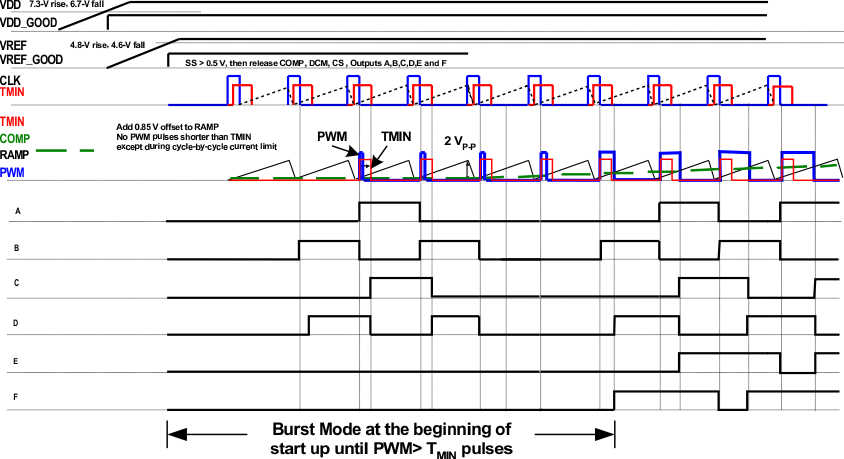
No output delay shown, COMP-to-RAMP offset not included.
There is no pulse on OUTE during burst mode at startup. Two falling edge PWM pulses are required before enabling the synchronous rectifier outputs. Narrower pulse widths (less than 50% duty cycle) may be observed in the first OUTD pulse of a burst. The user must design the bootstrap capacitor charging circuit of the gate driver device so that the first OUTC pulse is transmitted to the MOSFET gate in all cases. Transformer based gate driver circuits are not affected. This behavior is described in more detail in the application note, Gate Driver Design Considerations.
Figure 1. UCC28950 Startup Timing Diagram
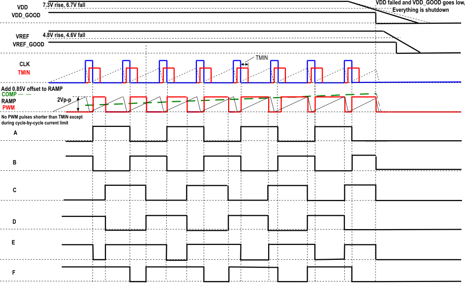
No output delay shown, COMP-to-RAMP offset not included.
Figure 2. UCC28950 Steady State/Shutdown Timing Diagram
6.8 Typical Characteristics
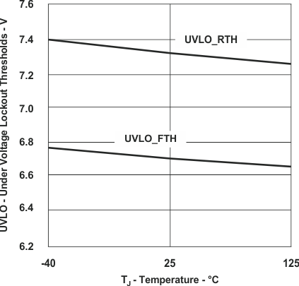 Figure 3. UVLO Thresholds vs Temperature
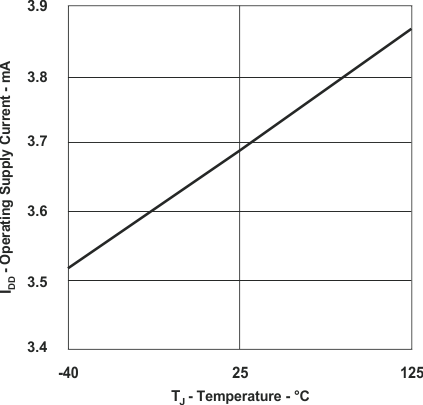 Figure 5. Supply Current vs Temperature
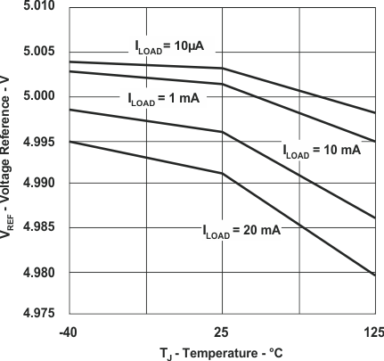 Figure 7. Voltage Reference (VDD = 12 V) vs Temperature
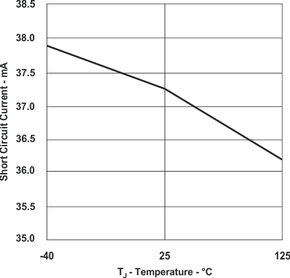 Figure 9. Short Circuit Current vs Temperature
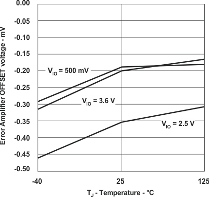 Figure 13. Error Amplifier Offset Voltage vs Temperature
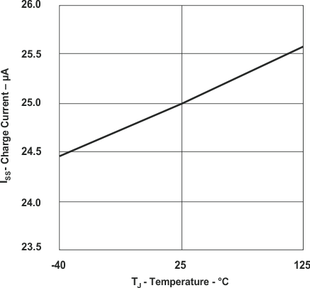 Figure 15. ISS Charge Current vs Temperature
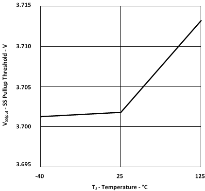 Figure 17. SS Pull-Up Threshold vs Temperature
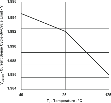 Figure 19. Current Sense Cycle-by-Cycle Limit vs Temperature
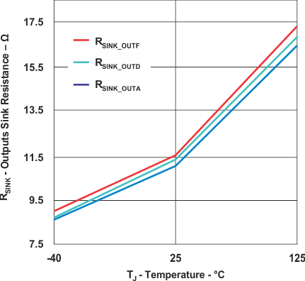 Figure 21. Outputs Sink Resistance vs Temperature
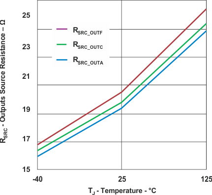 Figure 23. Outputs Source Resistance vs Temperature
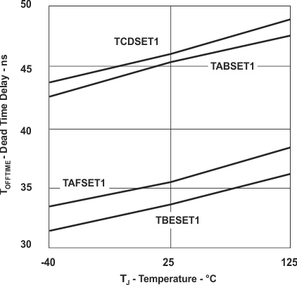 Figure 25. Dead Time Delay vs Temperature
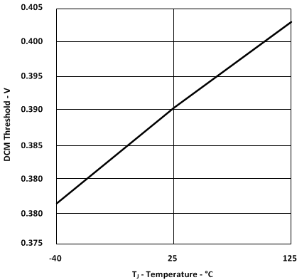 Figure 27. DCM Threshold vs Temperature
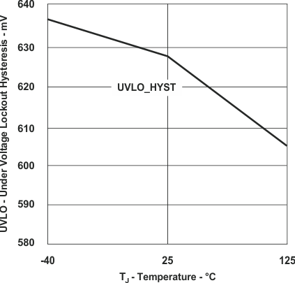 Figure 4. UVLO Hysteresis vs Temperature
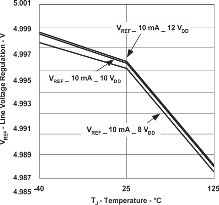 Figure 8. Line Voltage Regulation (ILOAD = 10 mA) vs Temperature
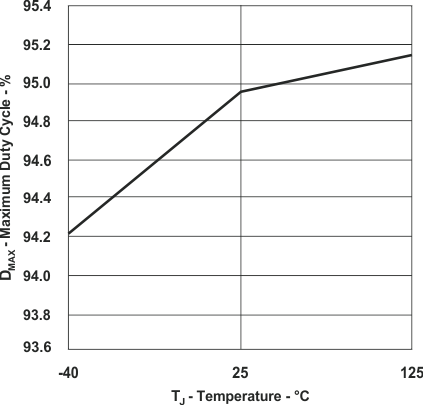 Figure 10. Maximum Duty Cycle vs Temperature
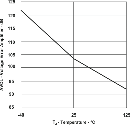 Figure 14. Voltage Error Amplifier (Open Loop Gain) vs Temperature
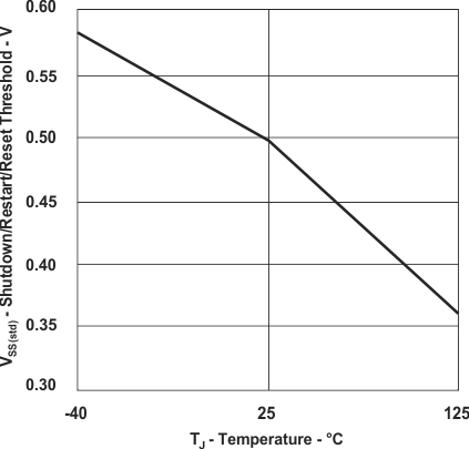 Figure 16. Shutdown/Restart/Reset Threshold vs Temperature
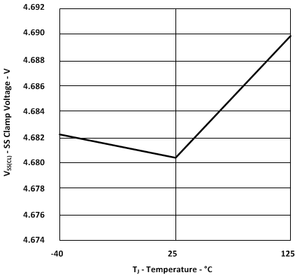 Figure 18. SS Clamp Voltage vs Temperature
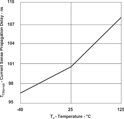 Figure 20. Current Sense Propagation Delay vs Temperature
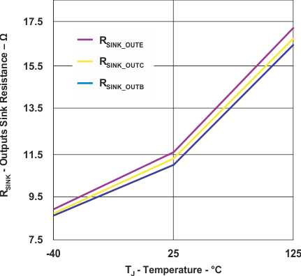 Figure 22. Outputs Sink Resistance vs Temperature
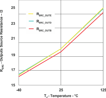 Figure 24. Outputs Source Resistance vs Temperature
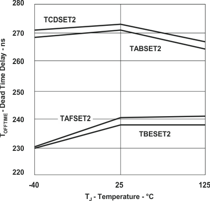 Figure 26. Dead Time Delay vs Temperature
