SLUSA16D March 2010 – November 2016 UCC28950
PRODUCTION DATA.
- 1 Features
- 2 Applications
- 3 Description
- 4 Revision History
- 5 Pin Configuration and Functions
- 6 Specifications
-
7 Detailed Description
- 7.1 Overview
- 7.2 Functional Block Diagram
- 7.3
Feature Description
- 7.3.1 Start-Up Protection Logic
- 7.3.2 Voltage Reference (VREF)
- 7.3.3 Error Amplifier (EA+, EA-, COMP)
- 7.3.4 Soft Start and Enable (SS/EN)
- 7.3.5 Light-Load Power Saving Features
- 7.3.6 Adaptive Delay, (Delay between OUTA and OUTB, OUTC and OUTD (DELAB, DELCD, ADEL))
- 7.3.7 Adaptive Delay (Delay between OUTA and OUTF, OUTB and OUTE (DELEF, ADELEF))
- 7.3.8 Minimum Pulse (TMIN)
- 7.3.9 Burst Mode
- 7.3.10 Switching Frequency Setting
- 7.3.11 Slope Compensation (RSUM)
- 7.3.12 Dynamic SR ON/OFF Control (DCM Mode)
- 7.3.13 Current Sensing (CS)
- 7.3.14 Cycle-by-Cycle Current Limit Current Protection and Hiccup Mode
- 7.3.15 Synchronization (SYNC)
- 7.3.16 Outputs (OUTA, OUTB, OUTC, OUTD, OUTE, OUTF)
- 7.3.17 Supply Voltage (VDD)
- 7.3.18 Ground (GND)
- 7.4 Device Functional Modes
-
8 Application and Implementation
- 8.1 Application Information
- 8.2
Typical Application
- 8.2.1 Design Requirements
- 8.2.2
Detailed Design Procedure
- 8.2.2.1 Power Loss Budget
- 8.2.2.2 Preliminary Transformer Calculations (T1)
- 8.2.2.3 QA, QB, QC, QD FET Selection
- 8.2.2.4 Selecting LS
- 8.2.2.5 Selecting Diodes DB and DC
- 8.2.2.6 Output Inductor Selection (LOUT)
- 8.2.2.7 Output Capacitance (COUT)
- 8.2.2.8 Select FETs QE and QF
- 8.2.2.9 Input Capacitance (CIN)
- 8.2.2.10 Current Sense Network (CT, RCS, R7, DA)
- 8.2.3 Application Curves
- 9 Power Supply Recommendations
- 10Layout
- 11Device and Documentation Support
- 12Mechanical, Packaging, and Orderable Information
10 Layout
10.1 Layout Guidelines
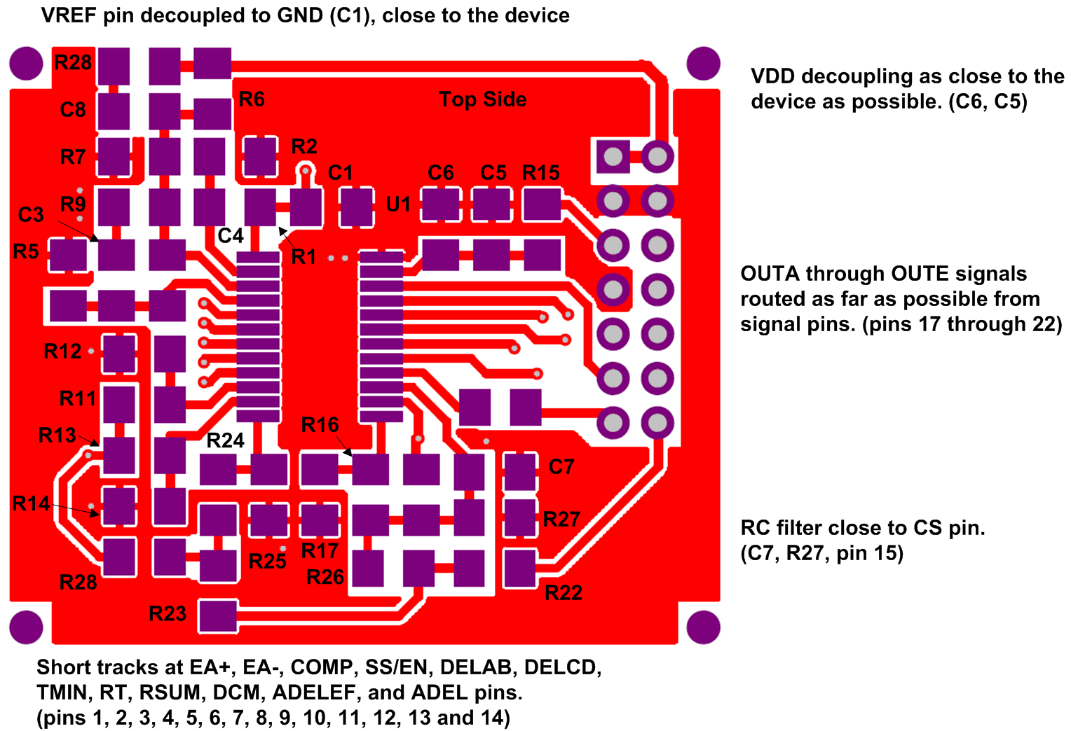
In order to increase the reliability and robustness of the design, TI recommends the following layout guidelines.
- VREF pin. Decouple this pin to GND with a good quality ceramic capacitor. A 1-uF, X7R, 25V capacitor is recommended. Keep VREF PCB tracks as far away as possible from sources of switching noise.
- EA+ pin. This is the non-inverting input to the error amplifier. It is a high impedance pin and is susceptible to noise pickup. Keep tracks from this pin as short as possible.
- EA– pin. This is the inverting input to the error amplifier. It is a high impedance pin and is susceptible to noise pickup. Keep tracks from this pin as short as possible.
- COMP pin. The error amplifier compensation network is normally connected to this pin. Keep tracks from this pin as short as possible.
- SS/EN pin. Keep tracks from this pin as short as possible. If the Enable signal is coming from a remote source then avoid running it close to any source of high dv/dt (MOSFET Drain connections for example) and add a simple RC filter at the SS/EN pin.
- DELAB, DELCD, DELEF, TMIN, RT, RSUM, DCM, ADELEF and ADEL pins. The components connected to these pins are used to set important operating parameters. Keep these components close to the IC and provide short, low impedance return connections to the GND pin.
- CS pin. This connection is arguably the most important single connection in the entire PSU system. Avoid running the CS signal traces near to sources of high dv/dt. Provide a simple RC filter as close to the pin as possible to help filter out leading edge noise spikes which will occur at the beginning of each switching cycle.
- SYNC pin. This pin is essentially a digital I/O port. If it is unused, then it may be left open circuit or tied to ground via a 1-kΩ resistor. If Synchronisation is used, then route the incoming Synchronisation signal as far away from noise sensitive input pins as possible.
- OUTA, OUTB, OUTC, OUTD, OUTE and OUTF pins. These are the gate drive output pins and will have a high dv/dt rate associated with their rising and falling edges. Keep the tracks from these pins as far away from noise sensitive input pins as possible. Ensure that the return currents from these outputs do not cause voltage changes in the analog ground connections to noise sensitive input pins. Follow the layout recommendation for Analog and Power ground Planes in Figure 45.
- VDD pin. This pin must be decoupled to GND using ceramic capacitors as detailed in the 'Power Supply Recommendations' section. Keep this capacitor as close to the VDD and GND pins as possible.
- GND pin. This pin provides the ground reference to the controller. Use a Ground Plane to minimize the impedance of the ground connection and to reduce noise pickup.
10.2 Layout Example
 Figure 65. UCC28950 Layout Example (Top Side)
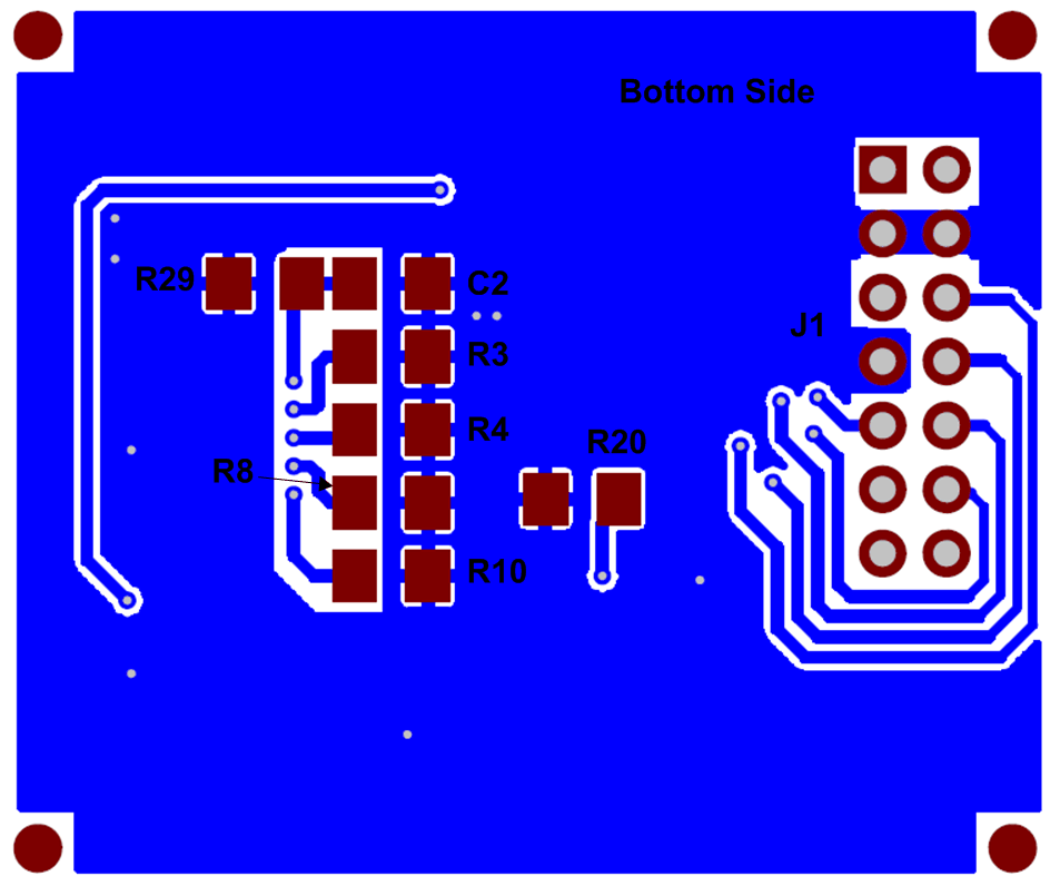
 Figure 66. UCC28950 Layout Example (Bottom Side)