ZHCSHY7A April 2018 – May 2018 UCC28742
PRODUCTION DATA.
- 1 特性
- 2 应用
- 3 说明
- 4 修订历史记录
- 5 Pin Configuration and Functions
- 6 Specifications
-
7 Detailed Description
- 7.1 Overview
- 7.2 Functional Block Diagram
- 7.3 Feature Description
- 7.4 Device Functional Modes
-
8 Applications and Implementation
- 8.1 Application Information
- 8.2
Typical Application
- 8.2.1 Design Requirements
- 8.2.2
Detailed Design Procedure
- 8.2.2.1 Custom Design With WEBENCH® Tools
- 8.2.2.2 VDD Capacitance, CDD
- 8.2.2.3 VDD Start-Up Resistance, RSTR
- 8.2.2.4 Input Bulk Capacitance and Minimum Bulk Voltage
- 8.2.2.5 Transformer Turns Ratio, Inductance, Primary-Peak Current
- 8.2.2.6 Transformer Parameter Verification
- 8.2.2.7 VS Resistor Divider and Line Compensation
- 8.2.2.8 Standby Power Estimate
- 8.2.2.9 Output Capacitance
- 8.2.2.10 Feedback Loop Design Consideration
- 8.2.3 Application Curves
- 8.3 Do's and Don'ts
- 9 Power Supply Recommendations
- 10Layout
- 11器件和文档支持
- 12机械、封装和可订购信息
5 Pin Configuration and Functions
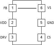
SOT23-6 Package
6-Pin DBV
Top View

Pin Functions
| PIN | I/O | DESCRIPTION | |
|---|---|---|---|
| NAME | NO. | ||
| CS | 4 | I | The current-sense (CS) input connects to a ground-referenced current-sense resistor in series with the power switch. The resulting voltage monitors and controls the peak primary current. A series resistor is added to this pin to compensate for peak switch current levels as the AC-mains input varies. |
| DRV | 3 | O | DRV is an output pin used to drive the gate of an external high voltage MOSFET switching transistor. |
| FB | 1 | I | The feedback (FB) input receives a current signal from the optocoupler output transistor. An internal current mirror divides the feedback current applies it to an internal pullup resistor to generate a control voltage, VCL. The voltage at this resistor directly drives the control law function, which determines the switching frequency and the peak amplitude of the switching current. |
| GND | 5 | G | The ground (GND) pin is both the reference pin for the controller, and the low-side return for the drive output. Special care must be taken to return all AC-decoupling capacitors as close as possible to this pin and avoid any common trace length with analog signal-return paths. |
| VDD | 2 | P | VDD is the bias supply input pin to the device. A carefully placed bypass capacitor to GND is required on this pin. Typical bypass capacitor values are from 0.047 µF to 10 µF depending on a design. |
| VS | 6 | I | Voltage sense (VS) is an input used to provide demagnetization timing feedback to the controller to limit frequency, to control constant-current operation, and to provide output-overvoltage detection. VS is also used for AC-mains input-voltage detection for peak primary-current compensation. This pin connects to a voltage divider between an auxiliary winding and GND. The value of the upper resistor of this divider programs the AC-mains run and stop thresholds, and factors into line compensation at the CS pin. |