ZHCSHY7A April 2018 – May 2018 UCC28742
PRODUCTION DATA.
- 1 特性
- 2 应用
- 3 说明
- 4 修订历史记录
- 5 Pin Configuration and Functions
- 6 Specifications
-
7 Detailed Description
- 7.1 Overview
- 7.2 Functional Block Diagram
- 7.3 Feature Description
- 7.4 Device Functional Modes
-
8 Applications and Implementation
- 8.1 Application Information
- 8.2
Typical Application
- 8.2.1 Design Requirements
- 8.2.2
Detailed Design Procedure
- 8.2.2.1 Custom Design With WEBENCH® Tools
- 8.2.2.2 VDD Capacitance, CDD
- 8.2.2.3 VDD Start-Up Resistance, RSTR
- 8.2.2.4 Input Bulk Capacitance and Minimum Bulk Voltage
- 8.2.2.5 Transformer Turns Ratio, Inductance, Primary-Peak Current
- 8.2.2.6 Transformer Parameter Verification
- 8.2.2.7 VS Resistor Divider and Line Compensation
- 8.2.2.8 Standby Power Estimate
- 8.2.2.9 Output Capacitance
- 8.2.2.10 Feedback Loop Design Consideration
- 8.2.3 Application Curves
- 8.3 Do's and Don'ts
- 9 Power Supply Recommendations
- 10Layout
- 11器件和文档支持
- 12机械、封装和可订购信息
7.3.3 Control Law
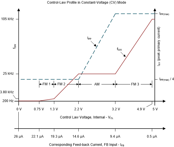
During voltage regulation (CV mode), the controller operates in frequency modulation mode and peak current amplitude modulation mode as illustrated in Figure 12 below. In CV mode operation, the control consists of four regions, namely, region FM 1, 2, AM and FM 3. The device internal VCL sets a particular region of operation. Refer to Figure 12 for VCL.
The device internally limits its operating frequency between fSW(min) and fSW(max), typically between 200 Hz and 105 kHz. The choice of transformer primary inductance and primary-peak current sets the maximum operating frequency of the converter, which must be equal to or lower than fSW(max). Conversely, the choice of maximum target operating frequency and primary-peak current determines the transformer primary-inductance value. The actual minimum switching frequency for any particular converter depends on several factors, including minimum loading level, leakage inductance losses, switch-node capacitance losses, other switching and conduction losses, and bias-supply requirements. In any case, the minimum steady-state frequency of the converter must always exceed fSW(min) or the output voltage may rise to the over-voltage protection level (OVP) and the controller responds as described in Fault Protection.
To achieve a regulated output voltage in the CV mode operation, energy balance has to be maintained. As the UCC28742 has a minimum switching frequency typical 200 Hz, together with the energy per switching cycle determined by converter parameters, such as the transformer primary inductance Lp and the selected RCS resistor, the converter has a minimum input power. A proper pre-load needs to be selected to ensure that this minimum energy is balanced during the no-load condition. The selection of the line compensation resistor value (RLC) connected to the CS pin can impact the energy per switching cycle based on low-line and high-line conditions. Typical Application section provides a design example to show how to implement these considerations.
 Figure 12. Frequency and Amplitude Modulation Modes
(during CV mode)
The steady-state control-law voltage, VCL, ranges between 0.75 V to 4.90 V. Heavy load operation is usually in Region FM 3 where frequency modulation to output regulation is used and primary-peak current is controlled at its maximum. The AM region is usually for medium-load range typically from 10% load and above. In this region switching frequency is fixed at nominal 25 kHz along with primary-peak current varying from 25% to 100% of its maximum. The low operating frequency ranges are for lighter loads to achieve stable regulation at low frequencies. In regions FM 1 and 2, peak-primary current is always maintained at IPP(max)/4. Transitions between levels are automatically accomplished by the controller depending on the internal control-law voltage, VCL and its corresponding FB pin current IFB. An internal frequency-dithering mechanism is enabled in Region FM 3 to reduce conducted EMI, and is disabled otherwise. The Wait state is enabled in regions FM 1, 2, and AM, refer to Figure 11.