ZHCSHY7A April   2018  – May 2018 UCC28742

PRODUCTION DATA.  

  1. 特性
  2. 应用
  3. 说明
    1.     Device Images
      1.      简化原理图
      2.      10W、5V 交流/直流转换器的典型效率
  4. 修订历史记录
  5. Pin Configuration and Functions
    1.     Pin Functions
  6. Specifications
    1. 6.1 Absolute Maximum Ratings
    2. 6.2 ESD Ratings
    3. 6.3 Recommended Operating Conditions
    4. 6.4 Thermal Information
    5. 6.5 Electrical Characteristics
    6. 6.6 Typical Characteristics
  7. Detailed Description
    1. 7.1 Overview
    2. 7.2 Functional Block Diagram
    3. 7.3 Feature Description
      1. 7.3.1 Detailed Pin Description
        1. 7.3.1.1 VDD (Device Bias Voltage Supply)
        2. 7.3.1.2 GND (Ground)
        3. 7.3.1.3 VS (Voltage-Sense)
        4. 7.3.1.4 DRV (Gate Drive)
        5. 7.3.1.5 CS (Current Sense)
        6. 7.3.1.6 FB (Feedback)
      2. 7.3.2 Secondary-Side Optically Coupled Constant-Voltage (CV) Regulation
      3. 7.3.3 Control Law
      4. 7.3.4 Constant Current Limit and Delayed Shutdown
      5. 7.3.5 Valley-Switching and Valley-Skipping
      6. 7.3.6 Start-Up Operation
      7. 7.3.7 Fault Protection
    4. 7.4 Device Functional Modes
  8. Applications and Implementation
    1. 8.1 Application Information
    2. 8.2 Typical Application
      1. 8.2.1 Design Requirements
      2. 8.2.2 Detailed Design Procedure
        1. 8.2.2.1  Custom Design With WEBENCH® Tools
        2. 8.2.2.2  VDD Capacitance, CDD
        3. 8.2.2.3  VDD Start-Up Resistance, RSTR
        4. 8.2.2.4  Input Bulk Capacitance and Minimum Bulk Voltage
        5. 8.2.2.5  Transformer Turns Ratio, Inductance, Primary-Peak Current
        6. 8.2.2.6  Transformer Parameter Verification
        7. 8.2.2.7  VS Resistor Divider and Line Compensation
        8. 8.2.2.8  Standby Power Estimate
        9. 8.2.2.9  Output Capacitance
        10. 8.2.2.10 Feedback Loop Design Consideration
      3. 8.2.3 Application Curves
    3. 8.3 Do's and Don'ts
  9. Power Supply Recommendations
  10. 10Layout
    1. 10.1 Layout Guidelines
    2. 10.2 Layout Example
  11. 11器件和文档支持
    1. 11.1 器件支持
      1. 11.1.1 开发支持
        1. 11.1.1.1 使用 WEBENCH® 工具创建定制设计
      2. 11.1.2 器件命名规则
        1. 11.1.2.1  电容术语(以法拉为单位)
        2. 11.1.2.2  占空比术语
        3. 11.1.2.3  频率术语(以赫兹为单位)
        4. 11.1.2.4  电流术语(以安培为单位)
        5. 11.1.2.5  电流和电压调节术语
        6. 11.1.2.6  变压器术语
        7. 11.1.2.7  功率术语(以瓦特为单位)
        8. 11.1.2.8  电阻术语(以 Ω 为单位)
        9. 11.1.2.9  时序术语(以秒为单位)
        10. 11.1.2.10 电压术语(以伏特为单位)
        11. 11.1.2.11 交流电压术语(以 VRMS 为单位)
        12. 11.1.2.12 效率术语
    2. 11.2 文档支持
      1. 11.2.1 相关文档
    3. 11.3 接收文档更新通知
    4. 11.4 社区资源
    5. 11.5 商标
    6. 11.6 静电放电警告
    7. 11.7 术语表
  12. 12机械、封装和可订购信息

封装选项

机械数据 (封装 | 引脚)
散热焊盘机械数据 (封装 | 引脚)
订购信息

Typical Application

Figure 18 illustrates a typical circuit diagram for AC-to-DC power conversion applications. It is a flyback converter with secondary-side regulation (SSR) controlled by UCC28742. Such applications widely exist in industrial and medical AC/DC power supplies, and also in ac-dc adapters, etc. The following sub-sections provide critical design formulas.
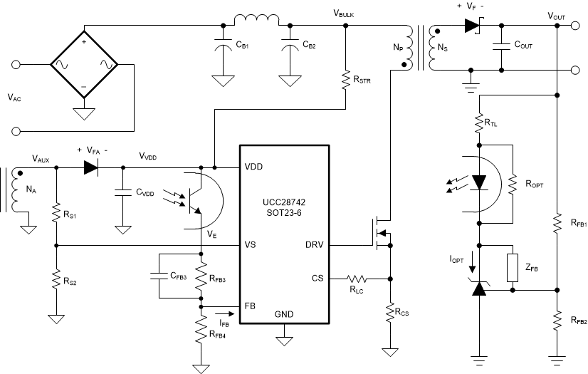
UCC28742 fig18_same_as_circuit_cover_page.gifFigure 18. Typical Application Circuit