SLUS544G September 2003 – April 2017 UCC28220 , UCC28221
PRODUCTION DATA.
- 1 Features
- 2 Applications
- 3 Description
- 4 Revision History
- 5 Device Comparison Table
- 6 Pin Configuration and Functions
- 7 Specifications
- 8 Detailed Description
- 9 Application and Implementation
- 10Power Supply Recommendations
- 11Layout
- 12Device and Documentation Support
- 13Mechanical, Packaging, and Orderable Information
封装选项
请参考 PDF 数据表获取器件具体的封装图。
机械数据 (封装 | 引脚)
- PW|16
- D|16
散热焊盘机械数据 (封装 | 引脚)
订购信息
8 Detailed Description
8.1 Overview
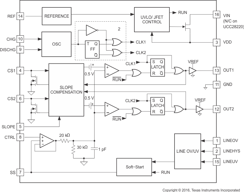
The UCC2822x device is comprised of several housekeeping blocks as well as two slope compensated PWM channels that are interleaved. The circuit is intended to run from an external VDD supply voltage between 8 V and 14 V; however, the UCC28221 has the addition of a high-voltage start-up JFET with control circuitry which can be used for system start-up. Other functions contained in the device are supply UVLO, 3.3-V reference, accurate line OV and UV functions, a high-speed programmable oscillator for both frequency and duty cycle, programmable slope compensation, and programmable soft-start functions.
The UCC2822x is a primary side controller for a two-channel interleaved power converter. The device is compatible with forward or flyback converters as long as a duty cycle clamp between 60% and 90% is required. The active clamp forward and flyback converters as well as the RCD and resonant reset forward converters are therefore compatible with this device. To ensure the two channels share the total converter output current, current mode control with internal slope compensation is used. Slope compensation is user programmable through a dedicated pin and can be set over a 50:1 range, ensuring good small-signal stability over a wide range of applications.
8.2 Functional Block Diagram

8.3 Feature Description
8.3.1 VDD
Because the driver output impedance is high, the energy storage requirement on the VDD capacitor is low. For improved noise immunity, TI recommends that the VDD pin is bypassed with a minimum of 0.1-µF capacitance to GND. In most typical applications, the bias voltage for the MOSFET drivers is also used as the VDD supply voltage for the chip. It is beneficial to add a low valued resistor between the bulk storage capacitor of the driver and the VDD capacitor for the UCC2822x. By adding a resistor in series with the bias supply with the bias supply, any noise that is present on the bias supply is filtered out before getting to the VDD pin of the controller.
8.3.2 Reference
For improved noise immunity, TI recommends that the reference pin, REF, is bypassed with a minimum of 0.1-µF capacitance to GND.
8.3.3 Oscillator Operation and Maximum Duty Cycle Setpoint
The oscillator uses an internal capacitor to generate the time base for both PWM channels. The oscillator is programmable over a 200-kHz to 2-MHz frequency range with 20% to 80% maximum duty cycle range. Both the dead time and the frequency of the oscillator are divided by 2 to generate the PWM clock and off-time information for each of the outputs. In this way, a 20% oscillator duty cycle corresponds to a 60% maximum duty cycle at each output, where an 80% oscillator duty cycle yields a 90% duty cycle clamp at each output.
The design equations for the oscillator and maximum duty cycle setpoint are given in Equation 1 through Equation 4.


where
- KOSC = 2.04 × 10¹⁰ (Ω/s)
- FOUT = Switching frequency at the outputs of the chip (Hz)
- DMAX(out) = Maximum duty cycle limit at the outputs of the chip
- DMAX(osc) = Maximum duty cycle of the oscillator for the desired maximum duty cycle at the outputs
- FOSC = Oscillator frequency for desired output frequency (Hz)
- RCHG = External oscillator resistor which sets the charge current (Ω)
- RDISCHG = External oscillator resistor which sets the discarge current (Ω)
8.3.4 Soft Start
A current is forced out of the SS pin, equal to 3/7 of the current set by RCHG, to provide a controlled ramp voltage. The current set by the RCHG resistor is equal to 2.5 V divided by RCHG. This ramp voltage overrides the commanded duty cycle on the CTRL pin, allowing a controlled start-up. Assuming the UCC288221 is biased on the primary side, the soft start must be quite quick to allow the secondary bias to be generated and the secondary side control can then take over. Once the soft-start time interval is complete, a closed-loop soft-start on the secondary side can be executed, such as Equation 5.

where
- ISS = current which is sourced out of the SS pin during the soft-start time (A)
8.3.5 Current Sense
The current sense signals CS1 and CS2 are level shifted by 0.5 V and have the slope compensation ramps added to them before being compared to the control voltage at the input of the PMW comparators. The amplitude of the current sense signal at full load must be selected such that it is very close to the maximum control voltage to limit the peak output current during short-circuit operation.
8.3.6 Output Drivers
The UCC2822x is intended to interface with the UCC2732x family of MOSFET drivers. As such, the output drive capability is low, effectively 100 Ω, and the driver output swing between GND and REF.
8.4 Device Functional Modes
8.4.1 Line Overvoltage and Undervoltage
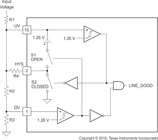
Three pins are provided to turn off the output drivers and reset the soft-start capacitor when the converter input voltage is outside a prescribed range. The undervoltage setpoint and undervoltage hysteresis are accurately set through external resistors. The overvoltage set point is also accurately set through a resistor ratio, but the hysteresis is fixed by the same resistor that set the undervoltage hysteresis.
Figure 17 and Figure 18 show the detailed functional diagram and operation of the undervoltage lockout (UVLO) and overvoltage lockout (OVLO) features. Equation 6 through Equation 9 are for setting the thresholds define in Figure 18.


 Figure 17. Line UVLO and OVLO Functional Diagram
 Figure 18. Line UVLO and OVLO Operation
The UVLO hysteresis and the OVLO hysteresis can be calculated as V2 – V1 and V4 – V3, respectively. By examining the design equations, it becomes apparent that the value of R4 sets the amount of hysteresis at both thresholds. By realizing this fact, the designer can then set the value of R4 based on the most critical hysteresis specification either at high line or at low line. In most designs the value of R4 is determined by the desired amount of hysteresis around the UVLO threshold. As an example, consider a telecom power supply with the following input UVLO and OVLO design specifications:
- V1 = 32 V
- V2 = 34 V
- V3 = 83 V
- V4 = 84.7 V
Then,
- R1 = 976 kΩ
- R2 = 24.9 kΩ
- R3 = 15 kΩ
- R4 = 604 kΩ
8.4.2 Start-Up JFET Section
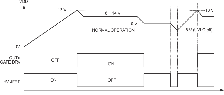
A 110-V start-up JFET is included to start the device from a wide range (36 V to 75 V) telecom input source. When VDD is lower than 13 V, the JFET is on, behaving as a current source charging the bias capacitors on VDD and supplying current to the device. In this way, the VDD bypass capacitors are charged to 13 V where the outputs start switching and the JFET is turned off. To enable a constant bias supply to the device during a pulse skipping condition, the JFET is turned back on whenever VDD decreases below 10 V and the outputs are not switching. Thus, the current from the JFET can overcome the internal bias currents, as long as the device is not actively switching the output drivers. See Figure 19 for a representation of the JFET and VDD operation. The OCC28220 does not contain an internal JFET and has a start-up threshold of 10 V which makes it capable of directly operating off a 12-V dc bus.
 Figure 19. JFET Device Operation With VDD Voltage
8.4.3 Slope Compensation
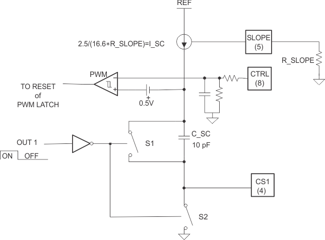
The slope compensation circuit in the UCC2822x operates on a cycle-by-cycle basis. The two channels have separate slope compensation circuits. These are fabricated in precisely the same way so as current sharing is unaffected by the slope compensation circuit. For each channel, an internal capacitor is reset whenever that channel's output is off. At the beginning of the PMW cycle, a current is mirrored off the SLOPE pin into the capacitor, developing an independent ramp. Because the two channel's ramps start when the channel's output changes from a low to high state, the ramps are thus interleaved. These internal ramps are added to the voltages on the current sense pins, CS1 and CS2, and form an input to the PMW comparators.
 Figure 20. Slope Compensation Detail for Chanel 1.
Duplicate Matched Circuitry Exists for Channel 2.
To ensure stability, the slope compensation circuit must add between 1/5 and 1 times the inductor downslope to each of the current sense signals before being applied to the input of the PWM comparator.