SLUS544G September 2003 – April 2017 UCC28220 , UCC28221
PRODUCTION DATA.
- 1 Features
- 2 Applications
- 3 Description
- 4 Revision History
- 5 Device Comparison Table
- 6 Pin Configuration and Functions
- 7 Specifications
- 8 Detailed Description
- 9 Application and Implementation
- 10Power Supply Recommendations
- 11Layout
- 12Device and Documentation Support
- 13Mechanical, Packaging, and Orderable Information
封装选项
请参考 PDF 数据表获取器件具体的封装图。
机械数据 (封装 | 引脚)
- PW|16
- D|16
散热焊盘机械数据 (封装 | 引脚)
订购信息
9 Application and Implementation
NOTE
Information in the following applications sections is not part of the TI component specification, and TI does not warrant its accuracy or completeness. TI’s customers are responsible for determining suitability of components for their purposes. Customers should validate and test their design implementation to confirm system functionality.
9.1 Application Information
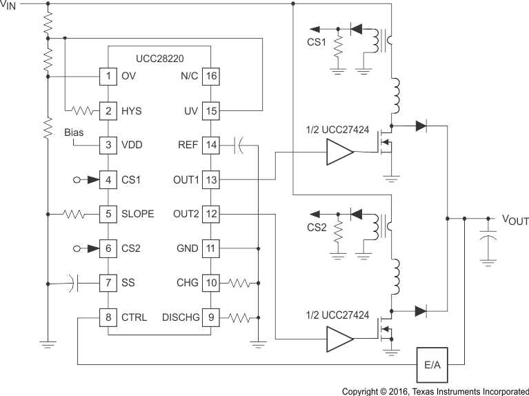
The UCC28220 control device from Texas Instruments is used in a dual-interleaved, forward converter that enables the power supply designer to reduce output current ripple and reduce magnetic size per power stage allowing for improved transient response. The UCC28220 is a dual-interleaved PWM controller with programmable maximum duty cycle per channel up to 90% for interleaved forward and interleaved flyback designs.
9.2 Typical Application
 Figure 21. Interleaved Boost Application Circuit Using the UCC28220
9.2.1 Design Requirements
Table 1 lists the design parameters for the interleaved boost application circuit.
Table 1. Design Parameters
| PARAMETER | MIN | TYP | MAX | UNIT |
|---|---|---|---|---|
| VIN | 85 | 110 or 230 | 265 | V RMS |
| VOUT | 374 | 390 | 425 | V |
| VRIPPLE | — | — | 30 | V |
| Current THD at 350 W | — | — | 10% | |
| PF at 350 W | 0.95 | — | — | |
| Full load efficiency | 90% | — | — | |
| fS | — | 100 | — | kHz |
| Holdup requirements, tHOLD | — | — | 20 | ms |
| fLINE | 47 | 50 | 60 | Hz |
9.2.2 Detailed Design Procedure
9.2.2.1 Overvoltage Protection and Undervoltage Lockout
The OVP function and undervoltage lockout (UVLO) were handled by the UCC28220. It is a simple comparator that monitors the boost voltage. The OVP for this design was set to 425 V and UVLO was set to 108 V. The preregulator does not start switching until VOUT reaches 108 V.
9.2.2.2 Peak Current Limit
Peak current limit is set by the maximum control voltage (VC) at the input of the UCC28220’s PWM comparator with Equation 10 through Equation 12. Where a is the current sense transformer turns ratio of T1 and T2. The peak current limit trip point was set for 130% of the nominal peak current to protect the boost FETs.


VC = 1.8, VCTRL was set to a maximum of 3 V to protect the UCC28220 CTRL pin.

Equation 12 considers slope compensation that is added later.
The peak current of the FET during power up is 2 times IPEAK under normal operation as calculated with Equation 13. This is due to the excessive slope compensation that is required for stability.

9.2.2.3 Current Sense Transformer Reset Resistor (T1 and T2)

9.2.2.4 Oscillator and Maximum Duty Cycle Clamp
The UCC28220’s oscillator and maximum duty cycle clamp are setup through resistor RCHG and discharge. The desired duty cycle clamp (DMAX) was set at 0.9 to stop the current sense transformers from saturating.

Equation 15 is UCC28220's oscillator constant.

Equation 16 is UCC28220's internal oscillator frequency.

Equation 17 is the internal duty cycle clamp.


9.2.3 Application Curves


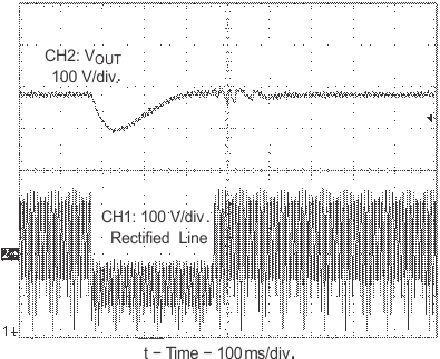
VIN stepped from 240 V to 120 V to 240 V