ZHCSTB0E February 2010 – November 2023 UCC27321-Q1 , UCC27322-Q1
PRODUCTION DATA
- 1
- 1 特性
- 2 应用
- 3 说明
- 4 说明(续)
- 5 Related Products
- 6 Pin Configuration and Functions
- 7 Specifications
- 8 Detailed Description
- 9 Application and Implementation
- 10Power Supply Recommendations
- 11Layout
- 12Device and Documentation Support
- 13Revision History
- 14Mechanical, Packaging, and Orderable Information
11.4 Power Dissipation
The UCC2732x-Q1 family of drivers are capable of delivering 9-A of current to a MOSFET gate for a period of several hundred nanoseconds. High peak current is required to turn an N-channel device ON quickly. Then, to turn the device OFF, the driver is required to sink a similar amount of current to ground. This repeats at the operating frequency of the power device. An N-channel MOSFET is used in this discussion because it is the most common type of switching device used in high-frequency power conversion equipment.
Design And Application Guide For High Speed MOSFET Gate Drive Circuits and Practical Considerations in High Performance MOSFET, IGBT and MCT Gate Drive Circuits contain detailed discussions of the drive current required to drive a power MOSFET and other capacitive-input switching devices. Much information is provided in tabular form to give a range of the current required for various devices at various frequencies. The information pertinent to calculating gate drive current requirements is summarized here.
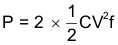
When a driver device is tested with a discrete, capacitive load it is a fairly simple matter to calculate the power that is required from the bias supply. The energy that must be transferred from the bias supply to charge the capacitor is given by Equation 8.

where
- C is the load capacitor
- V is the bias voltage feeding the driver
There is an equal amount of energy transferred to ground when the capacitor is discharged. This leads to a power loss given by Equation 9.
where
- f is the switching frequency
This power is dissipated in the resistive elements of the circuit. Thus, with no external resistor between the driver and gate, this power is dissipated inside the driver. Half of the total power is dissipated when the capacitor is charged, and the other half is dissipated when the capacitor is discharged. An example using the conditions of the previous gate-drive waveform helps to clarify this.
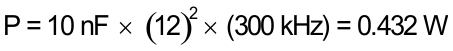
With VDD = 12 V, CLOAD = 10 nF, and f = 300 kHz, the power loss can be calculated as shown in Equation 11.
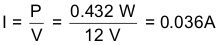
With a 12-V supply, this would equate, as shown in Equation 11, to a current of:
The switching load presented by a power MOSFETcan be converted to an equivalent capacitance by examining the gate charge required to switch the device. This gate charge includes the effects of the input capacitance plus the added charge required to swing the drain of the device between the ON and OFF states. Most manufacturers provide specifications that provide the typical and maximum gate charge, in nC, to switch the device under specified conditions. Using the gate charge Qg, one can determine the power that must be dissipated when charging a capacitor. This is done by using the equivalence Qg = CeffV to provide Equation 12 for power.
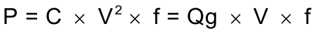
Equation 12 allows a power designer to calculate the bias power required to drive a specific MOSFET gate at a specific bias voltage.