ZHCSFN1A November 2016 – January 2022 UCC20520
PRODUCTION DATA
- 1 特性
- 2 应用
- 3 说明
- 4 Revision History
- 5 Pin Configuration and Functions
-
6 Specifications
- 6.1 Absolute Maximum Ratings
- 6.2 ESD Ratings
- 6.3 Recommended Operating Conditions
- 6.4 Thermal Information
- 6.5 Power Ratings
- 6.6 Insulation Specifications
- 6.7 Safety-Related Certifications
- 6.8 Safety-Limiting Values
- 6.9 Electrical Characteristics
- 6.10 Switching Characteristics
- 6.11 Insulation Characteristics Curves
- 6.12 Typical Characteristics
- 7 Parameter Measurement Information
- 8 Detailed Description
-
9 Application and Implementation
- 9.1 Application Information
- 9.2
Typical Application
- 9.2.1 Design Requirements
- 9.2.2
Detailed Design Procedure
- 9.2.2.1 Designing PWM Input Filter
- 9.2.2.2 Select External Bootstrap Diode and its Series Resistor
- 9.2.2.3 Gate Driver Output Resistor
- 9.2.2.4 Estimate Gate Driver Power Loss
- 9.2.2.5 Estimating Junction Temperature
- 9.2.2.6 Selecting VCCI, VDDA/B Capacitor
- 9.2.2.7 Dead Time Setting Guidelines
- 9.2.2.8 Application Circuits with Output Stage Negative Bias
- 9.2.2.9 56
- 9.2.3 Application Curves
- 10Layout
- 11Device and Documentation Support
9.2.2.3 Gate Driver Output Resistor
The external gate driver resistors, RON/ROFF, are used to:
- Limit ringing caused by parasitic inductances/capacitances.
- Limit ringing caused by high voltage/current switching dv/dt, di/dt, and body-diode reverse recovery.
- Fine-tune gate drive strength, i.e. peak sink and source current to optimize the switching loss.
- Reduce electromagnetic interference (EMI).
As mentioned in Section 8.3.4, the UCC20520 has a pull-up structure with a P-channel MOSFET and an additional pull-up N-channel MOSFET in parallel. The combined peak source current is 4 A. Therefore, the peak source current can be predicted with:
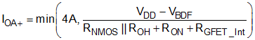
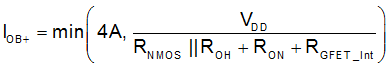
where
- RON: External turn-on resistance.
- RGFET_INT: Power transistor internal gate resistance, found in the power transistor datasheet.
- IO+ = Peak source current – The minimum value between 4 A, the gate driver peak source current, and the calculated value based on the gate drive loop resistance.
In this example:


Therefore, the high-side and low-side peak source current is 2.4 A and 2.5 A respectively. Similarly, the peak sink current can be calculated with:
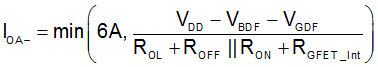
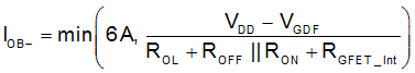
where
- ROFF: External turn-off resistance;
- VGDF: The anti-parallel diode forward voltage drop which is in series with ROFF. The diode in this example is an MSS1P4.
- IO-: Peak sink current – the minimum value between 6 A, the gate driver peak sink current, and the calculated value based on the gate drive loop resistance.
In this example,
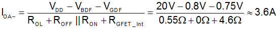
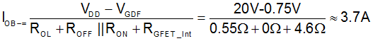
Therefore, the high-side and low-side peak sink current is 3.6 A and 3.7 A respectively.
Importantly, the estimated peak current is also influenced by PCB layout and load capacitance. Parasitic inductance in the gate driver loop can slow down the peak gate drive current and introduce overshoot and undershoot. Therefore, it is strongly recommended that the gate driver loop should be minimized. On the other hand, the peak source/sink current is dominated by loop parasitics when the load capacitance (CISS) of the power transistor is very small (typically less than 1 nF), because the rising and falling time is too small and close to the parasitic ringing period.