ZHCSFN1A November 2016 – January 2022 UCC20520
PRODUCTION DATA
- 1 特性
- 2 应用
- 3 说明
- 4 Revision History
- 5 Pin Configuration and Functions
-
6 Specifications
- 6.1 Absolute Maximum Ratings
- 6.2 ESD Ratings
- 6.3 Recommended Operating Conditions
- 6.4 Thermal Information
- 6.5 Power Ratings
- 6.6 Insulation Specifications
- 6.7 Safety-Related Certifications
- 6.8 Safety-Limiting Values
- 6.9 Electrical Characteristics
- 6.10 Switching Characteristics
- 6.11 Insulation Characteristics Curves
- 6.12 Typical Characteristics
- 7 Parameter Measurement Information
- 8 Detailed Description
-
9 Application and Implementation
- 9.1 Application Information
- 9.2
Typical Application
- 9.2.1 Design Requirements
- 9.2.2
Detailed Design Procedure
- 9.2.2.1 Designing PWM Input Filter
- 9.2.2.2 Select External Bootstrap Diode and its Series Resistor
- 9.2.2.3 Gate Driver Output Resistor
- 9.2.2.4 Estimate Gate Driver Power Loss
- 9.2.2.5 Estimating Junction Temperature
- 9.2.2.6 Selecting VCCI, VDDA/B Capacitor
- 9.2.2.7 Dead Time Setting Guidelines
- 9.2.2.8 Application Circuits with Output Stage Negative Bias
- 9.2.2.9 56
- 9.2.3 Application Curves
- 10Layout
- 11Device and Documentation Support
8.4.2.3

The steady state voltage at DT pin is around 0.8V, and the DT pin current will be less than 10uA when RDT=100kΩ. Therefore, It is recommended to parallel a ceramic capacitor, 2.2nF or above, with RDT to achieve better noise immunity and better deadtime matching between two channels, especially when the dead time is larger than 300ns. The major consideration is that the current through the RDT is used to set the dead time, and this current decreases as RDT increases.
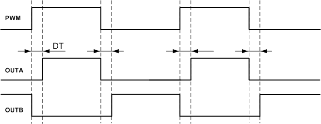
PWM input signal’s falling edge activates the programmed dead time for the other signal. The output signals’ dead time is always set to the driver’s programmed dead time. Various driver dead time logic operating conditions are illustrated and explained in Figure 8-4:
 Figure 8-4 Input and Output Logic Relationship with Dead Time