ZHCSFN1A November 2016 – January 2022 UCC20520
PRODUCTION DATA
- 1 特性
- 2 应用
- 3 说明
- 4 Revision History
- 5 Pin Configuration and Functions
-
6 Specifications
- 6.1 Absolute Maximum Ratings
- 6.2 ESD Ratings
- 6.3 Recommended Operating Conditions
- 6.4 Thermal Information
- 6.5 Power Ratings
- 6.6 Insulation Specifications
- 6.7 Safety-Related Certifications
- 6.8 Safety-Limiting Values
- 6.9 Electrical Characteristics
- 6.10 Switching Characteristics
- 6.11 Insulation Characteristics Curves
- 6.12 Typical Characteristics
- 7 Parameter Measurement Information
- 8 Detailed Description
-
9 Application and Implementation
- 9.1 Application Information
- 9.2
Typical Application
- 9.2.1 Design Requirements
- 9.2.2
Detailed Design Procedure
- 9.2.2.1 Designing PWM Input Filter
- 9.2.2.2 Select External Bootstrap Diode and its Series Resistor
- 9.2.2.3 Gate Driver Output Resistor
- 9.2.2.4 Estimate Gate Driver Power Loss
- 9.2.2.5 Estimating Junction Temperature
- 9.2.2.6 Selecting VCCI, VDDA/B Capacitor
- 9.2.2.7 Dead Time Setting Guidelines
- 9.2.2.8 Application Circuits with Output Stage Negative Bias
- 9.2.2.9 56
- 9.2.3 Application Curves
- 10Layout
- 11Device and Documentation Support
9.2.2.6.2 Selecting a VDDA (Bootstrap) Capacitor
A VDDA capacitor, also referred to as a bootstrap capacitor in bootstrap power supply configurations, allows for gate drive current transients up to 6 A, and needs to maintain a stable gate drive voltage for the power transistor.
The total charge needed per switching cycle can be estimated with
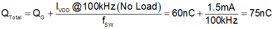
where
- QG: Gate charge of the power transistor.
- IVDD: The channel self-current consumption with no load at 100kHz.
Therefore, the absolute minimum CBoot requirement is:
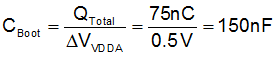
where
- ΔVVDDA is the voltage ripple at VDDA, which is 0.5 V in this example.
In practice, the value of CBoot is greater than the calculated value. This allows for the capacitance shift caused by the DC bias voltage and for situations where the power stage would otherwise skip pulses due to load transients. Therefore, it is recommended to include a safety-related margin in the CBoot value and place it as close to the VDD and VSS pins as possible. A 50-V 1-µF capacitor is chosen in this example.

To further lower the AC impedance for a wide frequency range, it is recommended to have bypass capacitor with a low capacitance value, in this example a 100 nF, in parallel with CBoot to optimize the transient performance.
Too large CBOOT is not good. CBOOT may not be charged within the first few cycles and VBOOT could stay below UVLO. As a result, the high-side FET does not follow input signal command. Also during initial CBOOT charging cycles, the bootstrap diode has highest reverse recovery current and losses.