ZHCSQX4F August   1995  – August 2022 UC1823A , UC1825A , UC2823A , UC2823B , UC2825A , UC2825B , UC3823A , UC3823B , UC3825A , UC3825B

PRODUCTION DATA  

  1. 1特性
  2. 2说明
  3. 3Revision History
  4. 4Ordering Information
  5. 5Pin Configuration and Functions
    1.     Terminal Functions
  6. 6Specifications
    1. 6.1 ABSOLUTE MAXIMUM RATINGS
    2. 6.2 Thermal Information
    3. 6.3 ELECTRICAL CHARACTERISTICS
    4. 6.4 ELECTRICAL CHARACTERISTICS
  7. 7Application and Implementation
    1. 7.1 LEADING EDGE BLANKING
    2. 7.2 UVLO、软启动和故障管理
    3. 7.3 ACTIVE LOW OUTPUTS DURING UVLO
    4. 7.4 CONTROL METHODS
    5. 7.5 SYNCHRONIZATION
    6. 7.6 HIGH CURRENT OUTPUTS
    7. 7.7 GROUND PLANES
    8. 7.8 OPEN LOOP TEST CIRCUIT
  8. 8Device and Documentation Support
    1. 8.1 Documentation Support
    2. 8.2 接收文档更新通知
    3. 8.3 支持资源
    4. 8.4 Trademarks
    5. 8.5 Electrostatic Discharge Caution
    6. 8.6 术语表
  9. 9Mechanical, Packaging, and Orderable Information

封装选项

请参考 PDF 数据表获取器件具体的封装图。

机械数据 (封装 | 引脚)
  • DW|16
散热焊盘机械数据 (封装 | 引脚)
订购信息

SYNCHRONIZATION

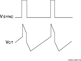
The oscillator can be synchronized by an external pulse inserted in series with the timing capacitor. Program the free running frequency of the oscillator to be 10% to 15% slower than the desired synchronous frequency. The pulse width should be greater than 10 ns and less than half the discharge time of the oscillator. The rising edge of the CLK/LEB pin can be used to generate a synchronizing pulse for other chips. Note that the CLK/LEB pin no longer accepts an incoming synchronizing signal.
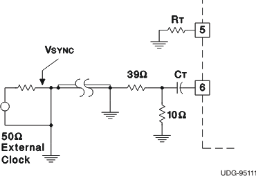
GUID-1542E4FC-050E-454D-BDCB-536200BDDF3C-low.gifFigure 7-6 General Oscillator Synchronization
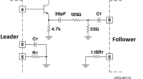
GUID-92BE8D6E-003E-4FC6-A137-4C5DC7E129A3-low.gifFigure 7-7 Two Unit Interface
GUID-903EF711-A06A-4B62-9E22-B4622FADB898-low.gifFigure 7-8 Operational Waveforms