SLUS557G March   2003  – December 2016 UC28023 , UC28025

PRODUCTION DATA.  

  1. Features
  2. Applications
  3. Description
  4. Revision History
  5. Pin Configuration and Functions
  6. Specifications
    1. 6.1 Absolute Maximum Ratings
    2. 6.2 ESD Ratings
    3. 6.3 Recommended Operating Conditions
    4. 6.4 Thermal Information
    5. 6.5 Electrical Characteristics
    6. 6.6 Switching Characteristics
    7. 6.7 Typical Characteristics
  7. Parameter Measurement Information
    1. 7.1 Control Methods and Test Circuits
  8. Detailed Description
    1. 8.1 Overview
    2. 8.2 Functional Block Diagram
    3. 8.3 Feature Description
      1. 8.3.1 Error Amplifier
      2. 8.3.2 Synchronization
      3. 8.3.3 Constant Volt-Second Clamp Circuit
      4. 8.3.4 Outputs
      5. 8.3.5 Open-Loop Laboratory Test Fixture
    4. 8.4 Device Functional Modes
  9. Application and Implementation
    1. 9.1 Application Information
    2. 9.2 Typical Application
      1. 9.2.1 Design Requirements
      2. 9.2.2 Detailed Design Procedure
        1. 9.2.2.1 Timing Resistor and Capacitor Selection
        2. 9.2.2.2 Turns Ratio Selection
        3. 9.2.2.3 Inductor Selection
        4. 9.2.2.4 Rectifier Diode Selection
        5. 9.2.2.5 Snubber Components Selection
        6. 9.2.2.6 VCC and VC Capacitor Selection
        7. 9.2.2.7 Output Capacitor Selection
        8. 9.2.2.8 Input Capacitor Selection
      3. 9.2.3 Application Curves
  10. 10Power Supply Recommendations
  11. 11Layout
    1. 11.1 Layout Guidelines
    2. 11.2 Layout Example
  12. 12Device and Documentation Support
    1. 12.1 Documentation Support
      1. 12.1.1 Related Documentation
    2. 12.2 Related Links
    3. 12.3 Receiving Notification of Documentation Updates
    4. 12.4 Community Resources
    5. 12.5 Trademarks
    6. 12.6 Electrostatic Discharge Caution
    7. 12.7 Glossary
  13. 13Mechanical, Packaging, and Orderable Information

封装选项

请参考 PDF 数据表获取器件具体的封装图。

机械数据 (封装 | 引脚)
  • DW|16
  • N|16
散热焊盘机械数据 (封装 | 引脚)
订购信息

Layout

Layout Guidelines

High speed circuits demand careful attention to layout and component placement. To assure proper performance of the UC2802x follow these rules:

  1. Use a ground plane.
  2. Damp or clamp parasitic inductive kick energy from the gate of driven MOSFETs. Do not allow the output pins to ring below ground. A series gate resistor or a shunt 1-A Schottky diode at the output pin serves this purpose.
  3. Bypass VCC, VC, and VREF. Use 0.1-µF monolithic ceramic capacitors with low equivalent series inductance. Allow less than 1 cm of total lead length for each capacitor between the bypassed pin and the ground plane.
  4. Treat the timing capacitor (CT) as a bypass capacitor.

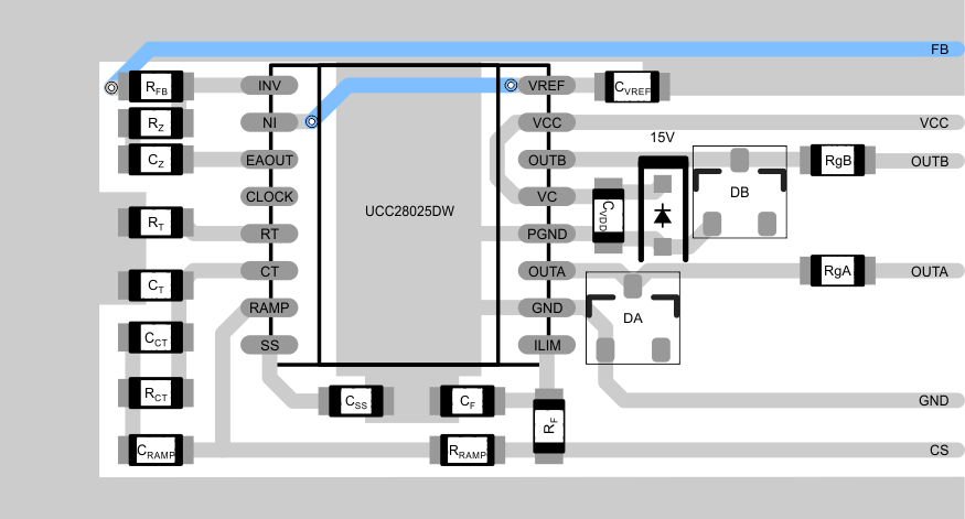
Layout Example

UC28023 UC28025 layout_slus557.gif Figure 21. Layout Recommendation