SLUS873C January 2009 – December 2016 UC1825A-SP
PRODUCTION DATA.
- 1 Features
- 2 Applications
- 3 Description
- 4 Revision History
- 5 Description (continued)
- 6 Pin Configuration and Functions
- 7 Specifications
- 8 Detailed Description
-
9 Application and Implementation
- 9.1 Application Information
- 9.2
Typical Application
- 9.2.1 Design Requirements
- 9.2.2
Detailed Design Procedure
- 9.2.2.1 Auxiliary Supply Voltage
- 9.2.2.2 Oscillator Frequency
- 9.2.2.3 Preliminary Considerations
- 9.2.2.4 Input Power
- 9.2.2.5 Primary Current
- 9.2.2.6 Sense Resistor R(s)
- 9.2.2.7 MOSFET DC Losses
- 9.2.2.8 Selection of Core Material
- 9.2.2.9 Main Transformer Design
- 9.2.2.10 Calculation of Transformer
- 9.2.2.11 Minimum Core Size
- 9.2.2.12 Core Loss Limited Conditions
- 9.2.2.13 Core Geometry Selection
- 9.2.2.14 Wire Size Selection
- 9.2.2.15 Calculate Secondary RMS Current
- 9.2.2.16 Transformer Assembly
- 9.2.2.17 Calculation of Winding Resistances and Losses
- 9.2.2.18 Transformer Power Losses
- 9.2.2.19 Output Section
- 9.2.2.20 UC1825A-SP PWM Control Section
- 9.2.2.21 Closing the Feedback Loop
- 9.2.2.22 Summary
- 9.2.3 Application Curves
- 10Power Supply Recommendations
- 11Layout
- 12Device and Documentation Support
- 13Mechanical, Packaging, and Orderable Information
封装选项
机械数据 (封装 | 引脚)
散热焊盘机械数据 (封装 | 引脚)
订购信息
8 Detailed Description
8.1 Overview
UC1825A-SP PWM controller is an improved version of the standard UC1825 family. Performance enhancements have been made to several of the circuit blocks. Error amplifier gain bandwidth product is
12 MHz, while input offset is 2 mV. Current limit threshold is assured to a tolerance of 5%. Oscillator discharge current is specified to 10 mA for accurate dead time control. Frequency accuracy is improved to 6%. Start-up supply current, typically 100 µA, is ideal for offline applications. The output drivers are redesigned to actively sink current during UVLO at no expense to the start-up current specifications. In addition, each output is capable of
2-A peak currents during transitions.
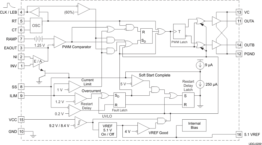
8.2 Functional Block Diagram
8.3 Feature Description
UC1825A-SP can be configured as current mode controller, used to support various topologies such as forward, flyback, Buck, Boost and using an external interface circuit will also support half-bridge, full bridge, and push-pull configurations.
8.3.1 Leading Edge Blanking
The UC1825A-SP performs fixed frequency pulse width modulation control. The UC1825A-SP outputs are alternately controlled. During every other cycle, one output is off. Each output then switches at one-half the oscillator frequency, varying in duty cycle from 0 to less than 50%.
To limit maximum duty cycle, the internal clock pulse blanks both outputs low during the discharge time of the oscillator. On the falling edge of the clock, the appropriate output is driven high. The end of the pulse is controlled by the PWM comparator, current limit comparator, or the overcurrent comparator.
Normally the PWM comparator senses a ramp crossing a control voltage (error amplifier output) and terminates the pulse. Leading edge blanking (LEB) causes the PWM comparator to be ignored for a fixed amount of time after the start of the pulse. This allows noise inherent with switched mode power conversion to be rejected. The PWM ramp input may not require any filtering as result of leading edge blanking.
To program a leading edge blanking (LEB) period, connect a capacitor, C, to CLK/LEB. The discharge time set by C and the internal 10-kΩ resistor determines the blanked interval. The 10-kΩ resistor has a 10% tolerance. For more accuracy, an external 2-kΩ 1% resistor (R) can be added, resulting in an equivalent resistance of 1.66 kΩ with a tolerance of 2.4%. The design equation is shown in Equation 1:

Values of R less than 2 kΩ must not be used.
Leading edge blanking is also applied to the current limit comparator (see Figure 3). After LEB, if the ILIM pin exceeds the 1-V threshold, the pulse is terminated. The overcurrent comparator, however, is not blanked. It catches catastrophic overcurrent faults without a blanking delay. Any time the ILIM pin exceeds 1.2 V, the fault latch is set and the outputs driven low. For this reason, some noise filtering may be required on the ILIM pin.
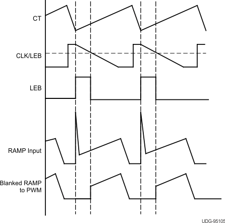 Figure 3. Leading Edge Blanking Operational Waveforms
8.3.2 UVLO, Soft-Start, and Fault Management
Soft-start is programmed by a capacitor on the SS pin. At power up, SS is discharged. When SS is low, the error amplifier output is also forced low. While the internal 9-μA source charges the SS pin, the error amplifier output follows until closed loop regulation takes over.
Anytime ILIM exceeds 1.2 V, the fault latch is set and the output pins are driven low, as shown in Figure 4. The soft-start cap is then discharged by a 250-μA current sink. No more output pulses are allowed until soft-start is fully discharged and ILIM is less than 1.2 V. At this point the fault latch resets and the chip executes a soft-start.
Should the fault latch get set during soft-start, the outputs are immediately terminated, but the soft-start capacitor does not discharge until it has been fully charged first. This results in a controlled hiccup interval for continuous fault conditions.
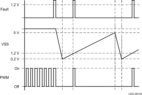 Figure 4. Soft-Start and Fault Waveforms
8.3.3 Active Low Outputs During UVLO
The UVLO function forces the outputs to be low and considers both VCC and VREF before allowing the chip to operate (see Figure 5 and Figure 6).
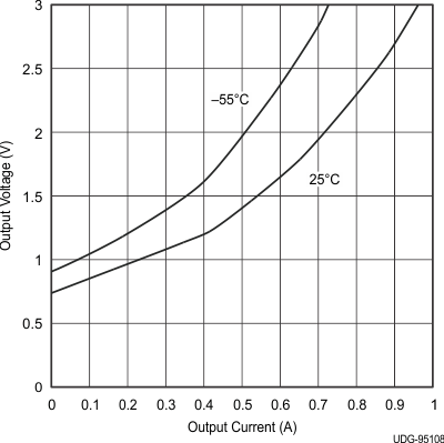 Figure 5. Output Voltage vs Output Current
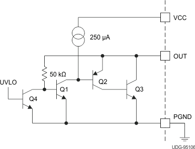 Figure 6. Output V And I During UVLO
8.3.5 Synchronization
The oscillator can be synchronized by an external pulse inserted in series with the timing capacitor (see Figure 8). Program the free running frequency of the oscillator to be 10% to 15% slower than the desired synchronous frequency. The pulse width must be greater than 10 ns and less than half the discharge time of the oscillator. Figure 9 shows how to synchronize two ICs, with one as master and one as slave. Figure 10 shows the waveforms in a master and slave configuration.
NOTE
The CLK/LEB pin no longer accepts an incoming synchronizing signal.
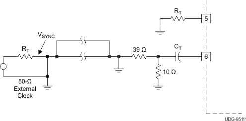 Figure 8. General Oscillator Synchronization
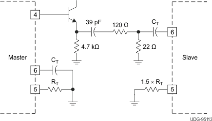 Figure 9. Two Unit Interface
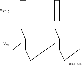 Figure 10. Operational Waveforms
8.3.6 High Current Outputs
Each totem pole output of the UC1825A-SP can deliver a 2-A peak current into a capacitive load. The output can slew a 1000-pF capacitor by 15 V in approximately 20 ns. Separate collector supply (VC) and power ground (PGND) pins help decouple the analog circuitry of the device from the high-power gate drive noise. The use of
3-A Schottky diodes (1N5120, USD245, or equivalent) as shown in the Figure 25 from each output to both VC and PGND are recommended. The diodes clamp the output swing to the supply rails, necessary with any type of inductive or capacitive load, typical of a MOSFET gate, as shown in Figure 11. Schottky diodes must be used because a low forward voltage drop is required.
NOTE
Do not use standard silicon diodes.
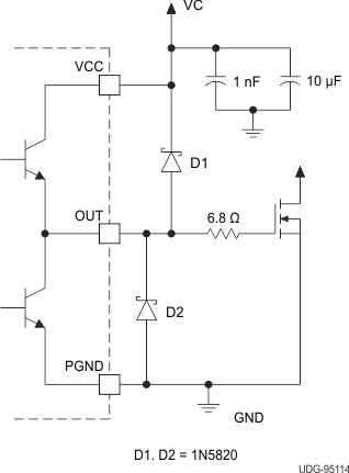 Figure 11. Power MOSFET Drive Circuit
8.3.7 Open Loop Test Circuit
This test fixture is useful for exercising many functions of this device family and measuring their specifications (see Figure 12). As with any wideband circuit, careful grounding and bypass procedures must be followed. TI highly recommends using a ground plane.
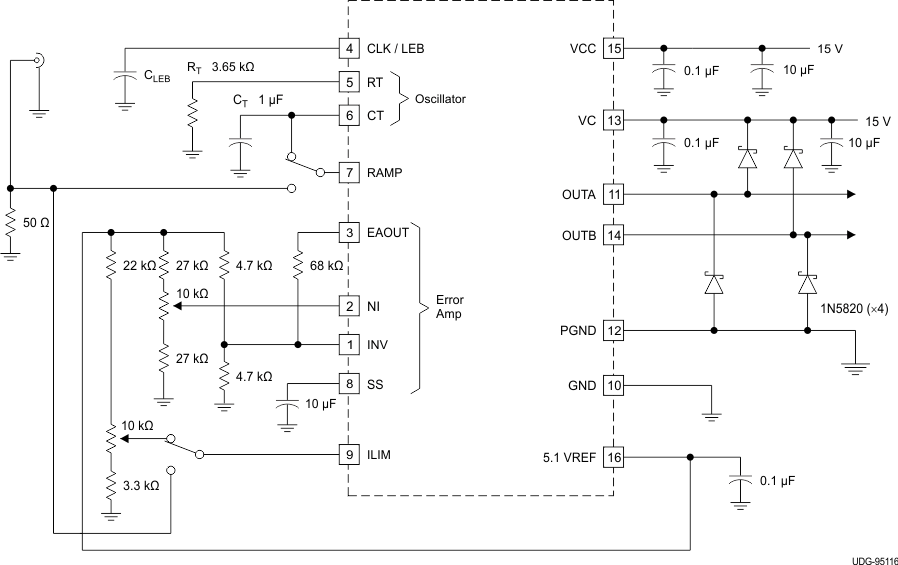 Figure 12. Open Loop Test Circuit Schematic
8.4 Device Functional Modes
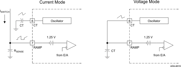
The UC1825A-SP is compatible with voltage-mode or current-mode topologies. The UC1825A-SP uses fixed frequency, peak current mode control. An internal oscillator initiates the turnon of the driver to high-side power switch. The external power switch current is sensed through an external resistor and is compared through internal comparator. The voltage generated at the COMP pin is stepped down through internal resistors (as shown in Functional Block Diagram). When the sensed current reaches the stepped down COMP voltage, the high-side power switch is turned off.
