ZHCSF18E May 2016 – May 2019 TUSB1002
PRODUCTION DATA.
- 1 特性
- 2 应用
- 3 说明
- 4 修订历史记录
- 5 Pin Configuration and Functions
- 6 Specifications
-
7 Detailed Description
- 7.1 Overview
- 7.2 Functional Block Diagram
- 7.3
Feature Description
- 7.3.1 4-Level Control Inputs
- 7.3.2 Linear Equalization
- 7.3.3 Adjustable VOD Linear Range and DC Gain
- 7.3.4 Receiver Detect Control
- 7.3.5 USB3.1 Dual Channel Operation (MODE = “F”)
- 7.3.6 USB3.1 Single Channel Operation (MODE = “1”)
- 7.3.7 PCIe/SATA/SATA Express Redriver Operation (MODE = “R”; CFG1 = "0"; CFG2 = "0" )
- 7.4 Device Functional Modes
- 7.5 U0 Mode
- 7.6 U1 Mode
- 7.7 U2/U3 Mode
- 8 Application and Implementation
- 9 Power Supply Recommendations
- 10Layout
- 11器件和文档支持
- 12机械、封装和可订购信息
6.9 Switching Characteristics
over operating free-air temperature range (unless otherwise noted)| PARAMETER | TEST CONDITIONS | MIN | TYP | MAX | UNIT | |
|---|---|---|---|---|---|---|
| USB3.1 Transmitter Interface (TX1P/N, TX2P/N) | ||||||
| tTX-RISE-FALL | Transmitter rise/fall time | 20% to 80% of differential output; 1200mVpp linear range setting | 40 | ps | ||
| tRF-MISMATCH | Transmitter rise/fall mismatch | 20% to 80% of differential output; 1200mVpp linear range setting; 1000mVpp VID; | 0.01 | UI | ||
| tTX-DJ | Residual deterministic jitter | @10Gbps; 1200mVpp Linear Range Setting | 0.08 | UI | ||
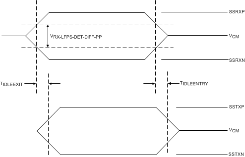
 Figure 1. Idle Entry and Exit Latency
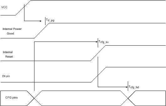
  Figure 2. Power-Up Diagram