ZHCS971B June 2012 – July 2016 TS3USB3200
PRODUCTION DATA.
8 Application and Implementation
NOTE
Information in the following applications sections is not part of the TI component specification, and TI does not warrant its accuracy or completeness. TI’s customers are responsible for determining suitability of components for their purposes. Customers should validate and test their design implementation to confirm system functionality.
8.1 Application Information
For Mobility Display Port Applications (MyDP) the signal voltage must be biased to ensure that the signal never exceeds the Recommended Operating Conditions for the TS3USB3200. Namely the VI/O must never operate outside the range of 0 V to 3.6 V.
The control pins (SEL1 and SEL2) have built-in 6-MΩ pulldown resistors to ensure the USB paths are enabled for TS3USB3200 and allow connectivity to the TSU5611 USB accessory switch.
8.2 Typical Applications
8.2.1 TS3USB3200 Configured to be Powered by VBUS Through the MicroUSB Connector
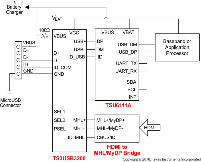
During manufacturing test when battery power is not available, the TS3USB3200 can be configured, as shown in Figure 10, to be powered by VBUS through the microUSB connector.
8.2.1.1 Design Requirements
Design requirements of the MHL and USB 1.0,1.1, and 2.0 standards must be followed. The TS3USB3200 has internal 6-MΩ pulldown resistors on SEL and OE, so no external resistors are required on the logic pins. The internal pulldown resistor on SEL ensures the USB channel is selected by default. The internal pulldown resistor on OE enables the switch when power is applied to VCC.
8.2.1.2 Detailed Design Procedure
The TS3USB3200 can be properly operated without any external components. However, TI recommends that unused pins must be connected to ground through a 50-Ω resistor to prevent signal reflections back into the device.
8.2.1.3 Application Curves
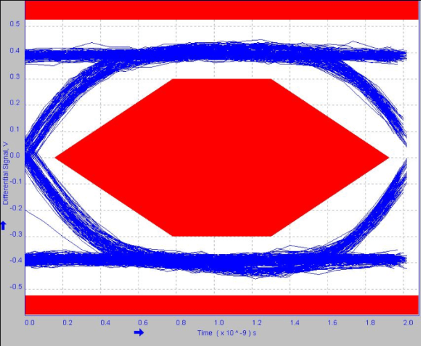 Figure 11. 480-Mbps USB 2.0 Eye Pattern With No Device
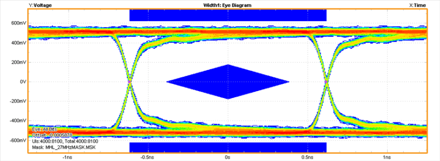 Figure 13. Eye Pattern: 0.7-Gbps MHL Eye Pattern for With No Device
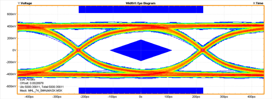 Figure 15. Eye Pattern: 2.2-Gbps MHL Eye Pattern for With No Device
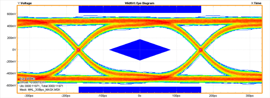 Figure 17. Eye Pattern: 3-Gbps MHL Eye Pattern for With No Device
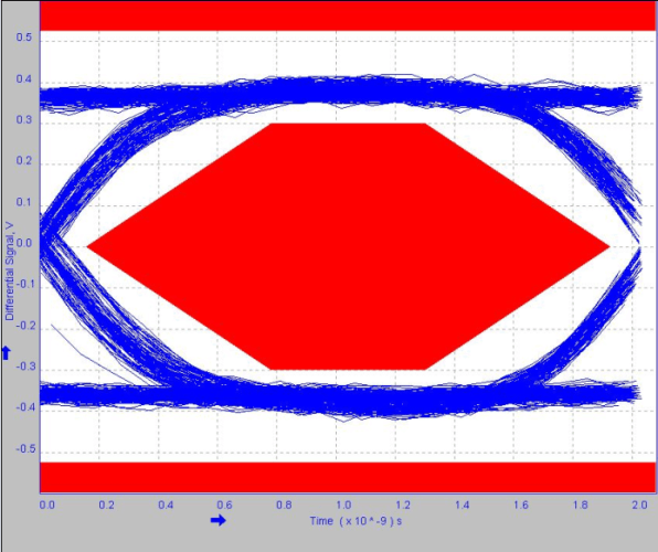 Figure 12. 480-Mbps USB 2.0 Eye Pattern for USB Switch
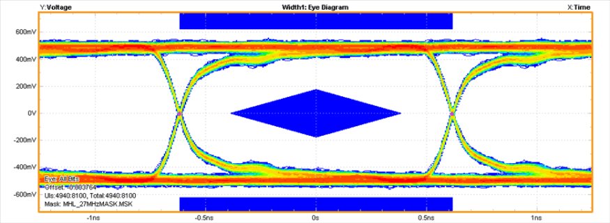 Figure 14. Eye Pattern: 0.7-Gbps MHL Eye Pattern for MHL Switch
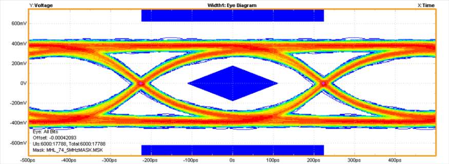 Figure 16. Eye Pattern: 2.2-Gbps MHL Eye Pattern for MHL Switch
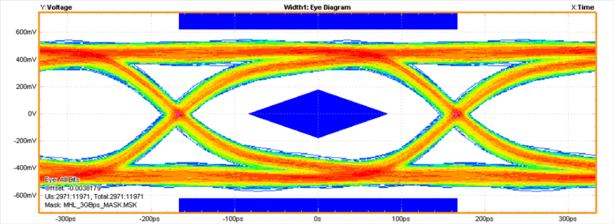 Figure 18. Eye Pattern: 3-Gbps MHL Eye Pattern for MHL Switch
8.2.2 TS3USB3200 Powered by Mobile Device’s Standalone Battery
The TS3USB3200 can also be powered by the mobile device’s standalone battery. Figure 19 shows a typical implementation. The VBUS pin of the TS3USB3200 can simply be grounded under such conditions.
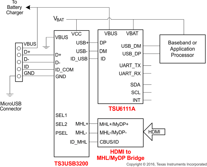 Figure 19. Typical Application Schematic Powered by Mobile Devices
8.2.2.1 Design Requirements
The TS3USB3200 can be properly operated without any external components. However, TI recommends that unused pins must be connected to ground through a 50-Ω resistor to prevent signal reflections back into the device.
8.2.2.2 Detailed Design Procedure
The VBUS pin of the TS3USB3200 can simply be grounded under such conditions.
