ZHCS971B June 2012 – July 2016 TS3USB3200
PRODUCTION DATA.
6 Specifications
6.1 Absolute Maximum Ratings
over operating free-air temperature range (unless otherwise noted)(1)(2)| MIN | MAX | UNIT | |||
|---|---|---|---|---|---|
| VCC ,VBUS | Supply voltage(3) | –0.3 | 5.5 | V | |
| VI/O | Input/Output DC voltage(3) | –0.5 | 5.5 | V | |
| IK | Input/Output port diode current | VI/O < 0 | –50 | mA | |
| VI | Digital input voltage range (SEL1, SEL2, PSEL) | –0.3 | 5.5 | V | |
| IIK | Digital logic input clamp current(3) | VI < 0 | –50 | mA | |
| ICC | Continuous current through VCC | 100 | mA | ||
| IGND | Continuous current through GND | –100 | mA | ||
| Tstg | Storage temperature | –65 | 150 | °C | |
(1) Stresses beyond those listed under Absolute Maximum Ratings may cause permanent damage to the device. These are stress ratings only, and functional operation of the device at these or any other conditions beyond those indicated under Recommended Operating Conditions is not implied. Exposure to absolute-maximum-rated conditions for extended periods may affect device reliability.
(2) The algebraic convention, whereby the most negative value is a minimum and the most positive value is a maximum.
(3) All voltages are with respect to ground, unless otherwise specified.
6.2 ESD Ratings
| VALUE | UNIT | |||
|---|---|---|---|---|
| V(ESD) | Electrostatic discharge | Human-body model (HBM), per ANSI/ESDA/JEDEC JS-001(1) | ±3500 | V |
| Charged-device model (CDM), per JEDEC specification JESD22-C101(2) | ±1000 | |||
(1) JEDEC document JEP155 states that 500-V HBM allows safe manufacturing with a standard ESD control process.
(2) JEDEC document JEP157 states that 250-V CDM allows safe manufacturing with a standard ESD control process.
6.3 Recommended Operating Conditions
| MIN | MAX | UNIT | ||
|---|---|---|---|---|
| VCC | Supply voltage | 2.7 | 4.3 | V |
| VBUS | VBUS Supply voltage | 4.3 | 5.5 | V |
| VI/O (USB)
VI/O (ID) |
Analog voltage for USB and ID signal path | 0 | 3.6 | V |
| VI/O (MHL) | Analog voltage for MHL signal path | 1.6 | 3.4 | V |
| VI | Digital input voltage (SEL1, SEL2, PSEL) | 0 | VCC | V |
| TRAMP (VCC) | Power supply ramp time requirement (VCC) | 100 | 1000 | μs/V |
| TRAMP (VBUS) | Power supply ramp time requirement (VBUS) | 100 | 1000 | μs/V |
| TA | Operating free-air temperature | –40 | 85 | ºC |
6.4 Thermal Information
| THERMAL METRIC(1) | TS3USB3200 | UNIT | |
|---|---|---|---|
| RSV (UQFN) | |||
| 16 PINS | |||
| RθJA | Junction-to-ambient thermal resistance(2) | 109.1 | °C/W |
| RθJC(top) | Junction-to-case (top) thermal resistance | 36 | °C/W |
| RθJB | Junction-to-board thermal resistance | 46.4 | °C/W |
| ψJT | Junction-to-top characterization parameter | 1 | °C/W |
| ψJB | Junction-to-board characterization parameter | 49.7 | °C/W |
(1) For more information about traditional and new thermal metrics, see the Semiconductor and IC Package Thermal Metrics application report.
(2) The package thermal impedance is calculated in accordance with JESD 51-7.
6.5 Electrical Characteristics
TA = –40°C to 85°C, Typical values are at VCC = 3.3 V, TA = 25°C, (unless otherwise noted)| PARAMETER | TEST CONDITIONS | MIN | TYP | MAX | UNIT | ||
|---|---|---|---|---|---|---|---|
| MHL SWITCH | |||||||
| RON | ON-state resistance | VCC = 2.7 V | VI/O = 1.6 V, ION = –8 mA | 5.7 | Ω | ||
| ΔRON | ON-state resistance match between + and – paths | VCC = 2.7 V | VI/O = 1.6 V, ION = –8 mA | 0.4 | Ω | ||
| RON (FLAT) | ON-state resistance flatness | VCC = 2.7 V | VI/O = 1.6 V to 3.4 V, ION = –8 mA | 1 | Ω | ||
| IOZ | OFF leakage current | VCC = 4.3 V | Switch OFF, VMHL+/MHL– = 1.6 V to 3.4 V, VD+/D– = 0 V |
–2 | 2 | µA | |
| IOFF | Power-off leakage current | VCC = 0 V | Switch ON or OFF, VMHL+/MHL– = 1.6 V to 3.4 V, VD+/D– = NC |
–10 | 10 | µA | |
| ION | ON leakage current | VCC = 4.3 V | Switch ON, VMHL+/MHL– = 1.6 V to 3.4 V, VD+/D– = NC |
–2 | 2 | µA | |
| USB SWITCH | |||||||
| RON | ON-state resistance | VCC = 2.7 V | VI/O = 0.4 V, ION = –8 mA | 4.6 | Ω | ||
| ΔRON | ON-state resistance match between + and – paths | VCC = 2.7 V | VI/O = 0.4 V, ION = –8 mA | 0.4 | Ω | ||
| RON (FLAT) | ON-state resistance flatness | VCC = 2.7 V | VI/O = 0 V to 0.4 V, ION = –8 mA | 1 | Ω | ||
| IOZ | OFF leakage current | VCC = 4.3 V | Switch OFF, VUSB+/USB– = 0 V to 4.3 V, VD+/D– = 0 V |
–2 | 2 | µA | |
| IOFF | Power-off leakage current | VCC = 0 V | Switch ON or OFF, VUSB+/USB– = 0 V to 4.3 V, VD+/D– = NC |
–10 | 10 | µA | |
| ION | ON leakage current | VCC = 4.3 V | Switch ON, VUSB+/USB– = 0 V to 4.3 V, VD+/D– = NC |
–2 | 2 | µA | |
| ID SWITCH | |||||||
| RON | ON-state resistance | VCC = 2.7 V | VI/O = 3.3 V, ION = –8 mA | 6.5 | Ω | ||
| ΔRON | ON-state resistance match between + and – paths | VCC = 2.7 V | VI/O = 3.3 V, ION = –8 mA | 0.4 | Ω | ||
| IOZ | OFF leakage current | VCC = 4.3 V | Switch OFF, VID_MHL/ID_USB = 0 V to 4.3 V, VID_COM = 0 V |
–1 | 1 | µA | |
| IOFF | Power-off leakage current | VCC = 0 V | Switch ON or OFF, VID_MHL/ID_USB = 0 V to 4.3 V, VID_COM = NC |
–10 | 10 | µA | |
| ION | ON leakage current | VCC = 4.3 V | Switch ON, VID_MHL/ID_USB = 0 V to 4.3 V, VID_COM = 0 V |
–1 | 1 | µA | |
| DIGITAL CONTROL INPUTS (SEL1, SEL2, PSEL) | |||||||
| VIH | Input logic high | VCC = 2.7 V to 4.3 V | 1.3 | V | |||
| VIL | Input logic low | VCC = 2.7 V to 4.3 V | 0.6 | V | |||
| IIN | Input leakage current | VCC = 4.3 V, VI/O = 0 V to 4.3 V, VIN = 0 V to 2 V | –10 | 10 | μA | ||
6.6 Dynamic Characteristics
TA = –40°C to 85°C, Typical values are at VCC = 3.3 V, TA = 25°C (unless otherwise noted)| PARAMETER | TEST CONDITIONS | MIN | TYP | MAX | UNIT | ||
|---|---|---|---|---|---|---|---|
| MHL(1)/USB/ ID SWITCH | |||||||
| tpd | Propagation Delay | RL = 50 Ω, CL = 5 pF | VCC = 2.7 V to 4.3 V | 0.1 | ns | ||
| tON | Turnon time | RL = 50 Ω, CL = 5 pF | VCC = 2.7 V to 4.3 V | 400 | ns | ||
| tOFF | Turnoff time | RL = 50 Ω, CL = 5 pF | VCC = 2.7 V to 4.3 V | 400 | ns | ||
| tSK(P) | Skew of opposite transitions of same output | VCC = 2.7 V or 3.3V | VCC = 2.7 V to 4.3 V | 0.1 | 0.2 | ns | |
| CON(MHL) | MHL path ON capacitance | VCC = 3.3 V, VI/O = 0 or 3.3 V, f = 240 MHz | Switch ON | 1.6 | pF | ||
| CON(USB) | USB path ON capacitance | VCC = 3.3 V, VI/O = 0 or 3.3 V, f = 240 MHz | Switch ON | 1.4 | pF | ||
| COFF(MHL) | MHL path OFF capacitance | VCC = 3.3 V, VI/O = 0 or 3.3 V, f = 240 MHz | Switch OFF | 1.4 | pF | ||
| COFF(USB) | USB path OFF capacitance | VCC = 3.3 V, VI/O = 0 or 3.3 V, f = 240 MHz | Switch OFF | 1.6 | pF | ||
| CI | Digital input capacitance | VCC = 3.3 V, VI = 0 or 2V | 2.2 | pF | |||
| OISO | OFF Isolation | VCC = 2.7 V to 4.3 V, RL = 50 Ω, f = 240 MHz |
Switch OFF | –37 | dB | ||
| XTALK | Crosstalk | VCC = 2.7 V to 4.3 V, RL = 50 Ω, f = 240 MHz |
Switch ON | –37 | dB | ||
| BW(MHL) | MHL path –3-dB bandwidth | VCC = 2.7 V to 4.3 V, RL = 50 Ω | Switch ON | 5.5 | GHz | ||
| BW(USB) | USB path –3-dB bandwidth | VCC = 2.7 V to 4.3 V, RL = 50 Ω | Switch ON | 5.5 | GHz | ||
| BW(ID) | ID path –3-dB bandwidth | VCC = 2.7 V to 4.3 V, RL = 50 Ω | Switch ON | 4 | GHz | ||
| SUPPLY | |||||||
| VBUS | VBUS Power supply voltage | 4.3 | 5.5 | V | |||
| VCC | Power supply voltage | 2.7 | 4.3 | V | |||
| ICC | Positive supply current | VCC = 4.3 V, VIN = VCC or GND, VI/O = 0 V | Switch ON or OFF | 40 | 70 | µA | |
| ICC, VBUS | Positive supply current (VBUS mode) | VCC = 0 V, VBUS = 5.5 V, VIN = VCC or GND, VI/O = 0 V | Switch ON or OFF | 50 | µA | ||
(1) Specified by Design
6.7 Typical Characteristics
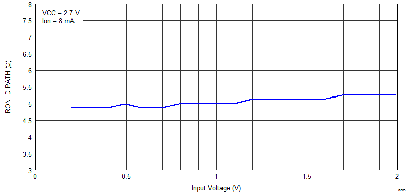 Figure 1. ON-Resistance vs VI for MHL Switch
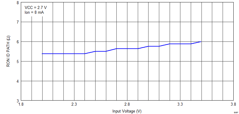
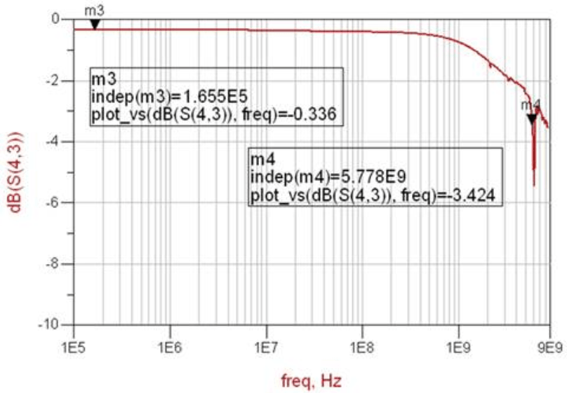 Figure 5. Gain vs Frequency for USB Switch
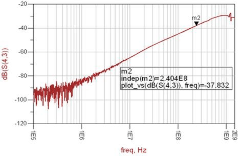 Figure 7. Off Isolation vs Frequency for USB Path
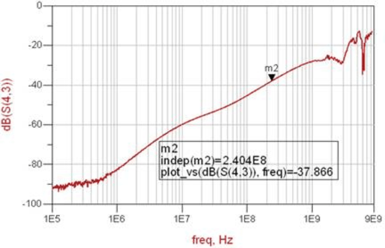 Figure 9. Crosstalk vs Frequency for USB Path
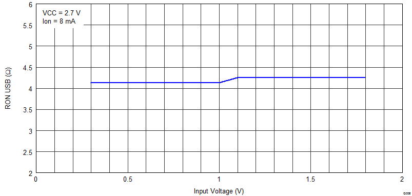 Figure 2. ON-Resistance vs VI for USB Switch
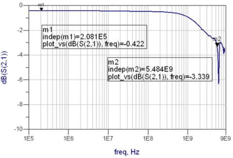 Figure 4. Gain vs Frequency for MHL Switch
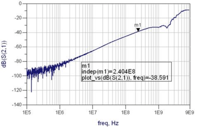
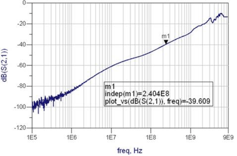 Figure 8. Crosstalk vs Frequency for MHL Path