ZHCSHH6B January 2018 – JANUARY 2019 TPSM846C24
PRODUCTION DATA.
- 1 特性
- 2 应用
- 3 说明
- 4 修订历史记录
- 5 Pin Configuration and Functions
- 6 Specifications
-
7 Detailed Description
- 7.1 Overview
- 7.2 Functional Block Diagram
- 7.3
Feature Description
- 7.3.1 Minimum Capacitance Requirements
- 7.3.2 Setting the Compensation Network
- 7.3.3 Transient Response
- 7.3.4 Setting the Output Voltage
- 7.3.5 Differential Remote Sense
- 7.3.6 Switching Frequency and Synchronization
- 7.3.7 Prebiased Output Start-Up
- 7.3.8 Power-Good (PGOOD) Indicator
- 7.3.9 Linear Regulators BP3 and BP6
- 7.3.10 Parallel Application
- 7.3.11 Parallel Operation
- 7.3.12 Overtemperature Protection
- 7.3.13 Overcurrent Protection
- 7.3.14 Output Overvoltage and Undervoltage Protection
- 7.4 Device Functional Modes
- 8 Application and Implementation
- 9 Power Supply Recommendations
- 10Layout
- 11器件和文档支持
- 12机械、封装和可订购信息
7.3.1 Minimum Capacitance Requirements
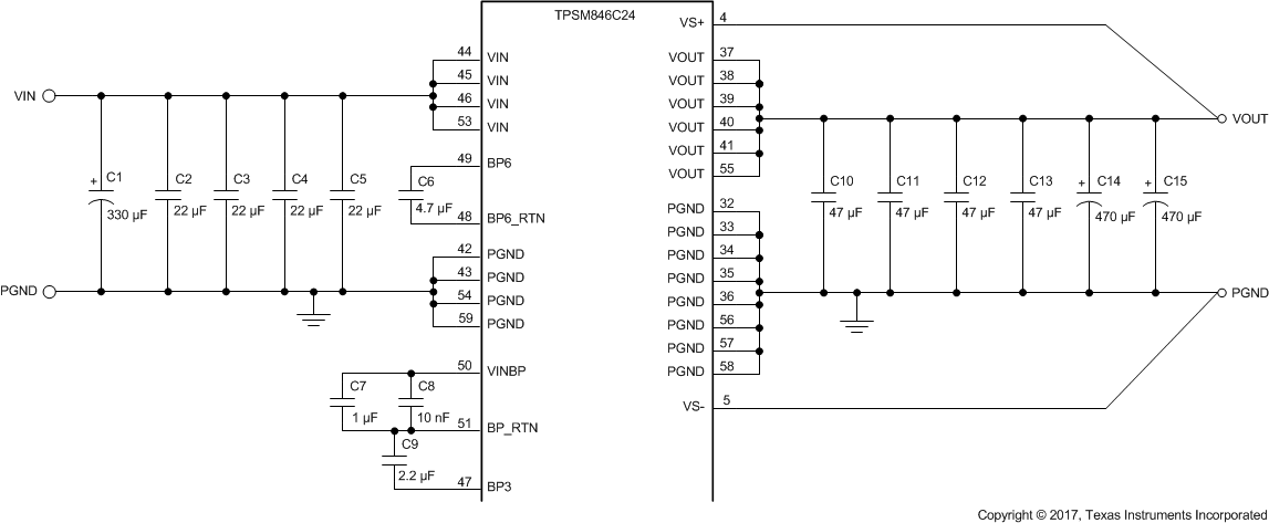
For proper operation, the minimum required input capacitance network consists of four 22-µF (or two 47-µF) ceramic capacitors plus a 330-µF bulk capacitor. See capacitors C1 thru C5 in Figure 13. Place the ceramic capacitors as close as possible to the VIN pins. The ground return path of the capacitors must connect to PGND pins 42, 43, 54, and 59 of the TPSM846C24.
The minimum required output capacitance network consists of four 47-µF (or two 100-µF) ceramic capacitors plus two 470-µF, low-ESR polymer capacitors. See capacitors C10 thru C15 in Figure 13. The combined ESR of the polymer capacitors must not be greater than 5 mΩ. Place the ceramic capacitors as close as possible to the VOUT and PGND pins of the module. This minimum network insures good transient response and minimal ripple amplitude. The total amount of output capacitance determines the values of the frequency compensation network. For more details see the Setting the Compensation Network section.
Additionally, the analog power path (VINBP) requires its own bypass network consisting of a 10-nF ceramic capacitor (C8 in Figure 13) and 1-µF ceramic capacitor (C7 in Figure 13) connected directly across pins 50 and 51 of the module. For proper operation, the two internal power supply rails of the module must also be bypassed. The 6.5-V rail (BP6) requires a 4.7-µF ceramic capacitor (C6 in Figure 13) placed across pins 48 and 49 of the module with short, direct traces. The 3.3-V rail (BP3) requires a 2.2-µF ceramic capacitor (C9 in Figure 13) placed very close to pins 47 and 51.
 Figure 13. Required Capacitor Schematic