ZHCSHL0C June   2019  – May 2022 TPS745-Q1

PRODUCTION DATA  

  1. 特性
  2. 应用
  3. 说明
  4. Revision History
  5. Pin Configuration and Functions
  6. Specifications
    1. 6.1 Absolute Maximum Ratings
    2. 6.2 ESD Ratings
    3. 6.3 Recommended Operating Conditions
    4. 6.4 Thermal Information
    5. 6.5 Electrical Characteristics
    6. 6.6 Timing Requirements
    7. 6.7 Typical Characteristics
  7. Detailed Description
    1. 7.1 Overview
    2. 7.2 Functional Block Diagrams
    3. 7.3 Feature Description
      1. 7.3.1 TPS745-Q1 Comparison
      2. 7.3.2 Undervoltage Lockout (UVLO)
      3. 7.3.3 Shutdown
      4. 7.3.4 Foldback Current Limit
      5. 7.3.5 Thermal Shutdown
    4. 7.4 Device Functional Modes
      1. 7.4.1 Device Functional Mode Comparison
      2. 7.4.2 Normal Operation
      3. 7.4.3 Dropout Operation
      4. 7.4.4 Disabled
  8. Application and Implementation
    1. 8.1 Application Information
      1. 8.1.1 Adjustable Device Feedback Resistors
      2. 8.1.2 Input and Output Capacitor Selection
      3. 8.1.3 Dropout Voltage
      4. 8.1.4 Exiting Dropout
      5. 8.1.5 Reverse Current
      6. 8.1.6 Power Dissipation (PD)
      7. 8.1.7 Power-Good Function
      8. 8.1.8 Feed-Forward Capacitor (CFF)
      9. 8.1.9 Start-Up Sequencing
    2. 8.2 Typical Application
      1. 8.2.1 Design Requirements
      2. 8.2.2 Detailed Design Procedure
        1. 8.2.2.1 Input Current
        2. 8.2.2.2 Thermal Dissipation
      3. 8.2.3 Application Curves
  9. Power Supply Recommendations
  10. 10Layout
    1. 10.1 Layout Guidelines
    2. 10.2 Layout Examples
  11. 11Device and Documentation Support
    1. 11.1 Device Support
      1. 11.1.1 Device Nomenclature
    2. 11.2 Documentation Support
      1. 11.2.1 Related Documentation
    3. 11.3 接收文档更新通知
    4. 11.4 支持资源
    5. 11.5 Trademarks
    6. 11.6 Electrostatic Discharge Caution
    7. 11.7 术语表
      1.      Mechanical, Packaging, and Orderable Information

封装选项

机械数据 (封装 | 引脚)
散热焊盘机械数据 (封装 | 引脚)
订购信息

Adjustable Device Feedback Resistors

Figure 8-1 shows that the output voltage of the TPS745P-Q1 can be adjusted from 0.55 V to 5.5 V by using a resistor divider network.
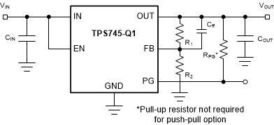
GUID-551B47D9-D0D3-43B5-AB40-85F291EF26DD-low.gifFigure 8-1 Adjustable Operation

The adjustable-version device requires external feedback divider resistors to set the output voltage. VOUT is set using the feedback divider resistors, R1 and R2, according to the following equation:

Equation 2. VOUT = VFB × (1 + R1 / R2)

To ignore the FB pin current error term in the VOUT equation, set the feedback divider current to 100x the FB pin current listed in the Electrical Characteristics table. This setting provides the maximum feedback divider series resistance, as shown in the following equation:

Equation 3. R1 + R2 ≤ VOUT / (IFB × 100)