ZHCSHL0C June   2019  – May 2022 TPS745-Q1

PRODUCTION DATA  

  1. 特性
  2. 应用
  3. 说明
  4. Revision History
  5. Pin Configuration and Functions
  6. Specifications
    1. 6.1 Absolute Maximum Ratings
    2. 6.2 ESD Ratings
    3. 6.3 Recommended Operating Conditions
    4. 6.4 Thermal Information
    5. 6.5 Electrical Characteristics
    6. 6.6 Timing Requirements
    7. 6.7 Typical Characteristics
  7. Detailed Description
    1. 7.1 Overview
    2. 7.2 Functional Block Diagrams
    3. 7.3 Feature Description
      1. 7.3.1 TPS745-Q1 Comparison
      2. 7.3.2 Undervoltage Lockout (UVLO)
      3. 7.3.3 Shutdown
      4. 7.3.4 Foldback Current Limit
      5. 7.3.5 Thermal Shutdown
    4. 7.4 Device Functional Modes
      1. 7.4.1 Device Functional Mode Comparison
      2. 7.4.2 Normal Operation
      3. 7.4.3 Dropout Operation
      4. 7.4.4 Disabled
  8. Application and Implementation
    1. 8.1 Application Information
      1. 8.1.1 Adjustable Device Feedback Resistors
      2. 8.1.2 Input and Output Capacitor Selection
      3. 8.1.3 Dropout Voltage
      4. 8.1.4 Exiting Dropout
      5. 8.1.5 Reverse Current
      6. 8.1.6 Power Dissipation (PD)
      7. 8.1.7 Power-Good Function
      8. 8.1.8 Feed-Forward Capacitor (CFF)
      9. 8.1.9 Start-Up Sequencing
    2. 8.2 Typical Application
      1. 8.2.1 Design Requirements
      2. 8.2.2 Detailed Design Procedure
        1. 8.2.2.1 Input Current
        2. 8.2.2.2 Thermal Dissipation
      3. 8.2.3 Application Curves
  9. Power Supply Recommendations
  10. 10Layout
    1. 10.1 Layout Guidelines
    2. 10.2 Layout Examples
  11. 11Device and Documentation Support
    1. 11.1 Device Support
      1. 11.1.1 Device Nomenclature
    2. 11.2 Documentation Support
      1. 11.2.1 Related Documentation
    3. 11.3 接收文档更新通知
    4. 11.4 支持资源
    5. 11.5 Trademarks
    6. 11.6 Electrostatic Discharge Caution
    7. 11.7 术语表
      1.      Mechanical, Packaging, and Orderable Information

封装选项

机械数据 (封装 | 引脚)
散热焊盘机械数据 (封装 | 引脚)
订购信息

Typical Characteristics

at operating temperature range TJ = 25°C, VIN = VOUT(NOM) + 0.5 V or 1.5 V (whichever is greater), IOUT = 1 mA, VEN = VIN, and CIN = COUT = 1 µF (unless otherwise noted)
GUID-07A1989C-BF78-475B-9BFB-BB833B02A849-low.gif
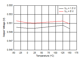
VOUT = 0.55 V, IOUT = 1 mA
Figure 6-1 Output Voltage vs Ambient Temperature
GUID-0DEE4C5C-17DD-4D40-9C94-13D49916E3A0-low.gif
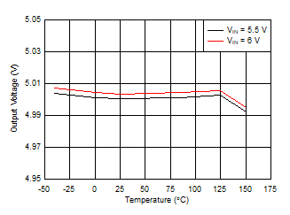
VOUT = 5 V, IOUT = 1 mA
Figure 6-3 Output Voltage vs Ambient Temperature
GUID-41AADBB2-C6AD-4210-BB45-62E7A89167B2-low.gif
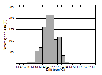
0.65-V, 3.3-V, and 5-V options, IOUT = 1 mA
Figure 6-5 Temperature Drift Histogram (25°C to 150°C)
GUID-D85087F7-55A7-4A5D-840C-9AF0E99FE4D8-low.gif
VOUT = 0.55 V, IOUT = 1 mA
Figure 6-7 0.55-V Line Regulation vs VIN
GUID-15AD6D28-4FD7-4B68-9B5C-3C6DBD1D6B2E-low.gif
Figure 6-9 3.3-V Dropout Voltage vs IOUT
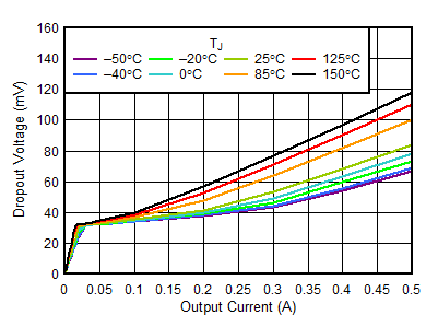
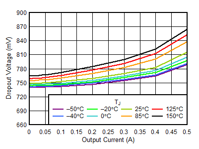
GUID-7B01E915-AE0B-4EB0-902F-C4BABF7605CC-low.gif
 
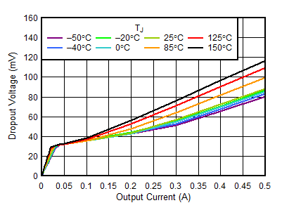
Figure 6-11 5.5-V Dropout Voltage vs IOUT
GUID-E56BBCC2-1682-4E39-98E2-2A8E27967B6A-low.gif
 
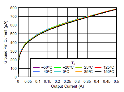
Figure 6-13 IGND vs IOUT
GUID-B80EDBF4-FCB5-4A1E-BD86-90EBE7956B5D-low.gif
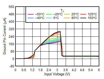
VOUT = 3.3 V, IOUT = 0 mA
Figure 6-15 IQ vs VIN
GUID-69FDA44D-E31A-4B2B-A765-9A48C638EFF7-low.gif
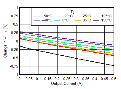
VIN = 2 V, VOUT = 0.55 V
Figure 6-17 0.55-V Load Regulation vs IOUT
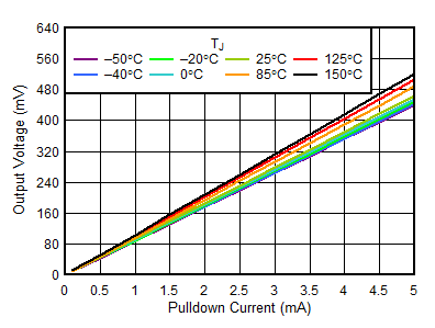
GUID-58A3BAC2-2772-4496-A2D3-DE388BB58644-low.gif
 
Figure 6-19 VOUT vs IOUT Pulldown Resistor
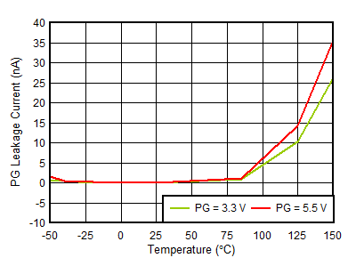
GUID-0F3231F8-E37A-4F9B-AC4A-0E3E9035BEFF-low.gif
 
Figure 6-21 IIkg(PG) vs Temperature and PG Pin Voltage
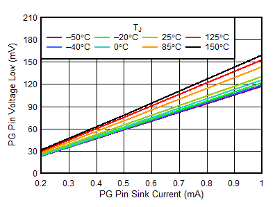
GUID-8D5D7814-2382-456C-A9BF-9AC9030B53EA-low.gif
VIN = 1.5 V, VOUT = 0.55 V
Figure 6-23 VOL(PG) vs PG Pin Sink Current
GUID-1E78C726-1DCF-450F-B7B9-1B708DC7907E-low.gif
B version
Figure 6-25 tPGDH vs Temperature (For TPS746B Only)
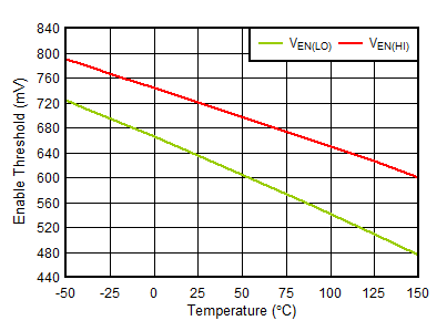
GUID-536B27E4-17DE-4BFA-9D1F-E47291C9BF30-low.gif
 
Figure 6-27 VEN(HI) and VEN(LO) vs Temperature
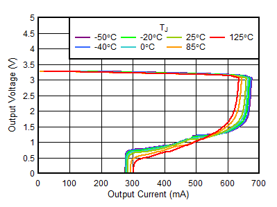
GUID-BAEA2BB2-4ECF-49D8-81B2-F2EE24CA642F-low.gif
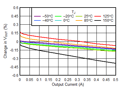
Figure 6-29 3.3-V VOUT vs IOUT
GUID-85944DC4-A826-486E-8211-C65B034F5895-low.gif
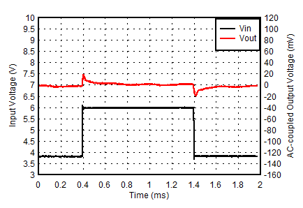
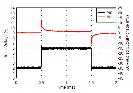
VOUT = 3.3 V, IOUT = 1 mA, VIN slew rate = 1 V/µs
Figure 6-31 3.3-V Line Transient
GUID-BAA29233-0160-4226-A2C7-9CE1ABA39A16-low.gif
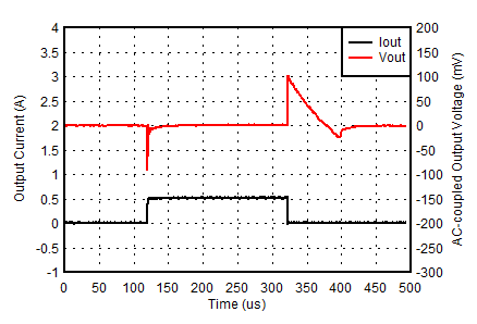
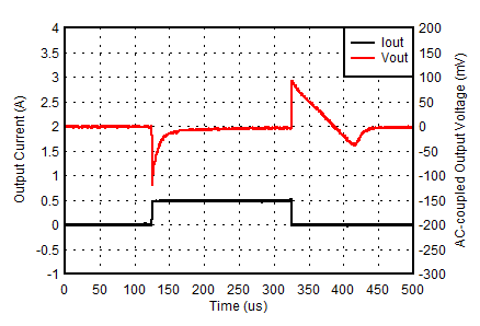
VIN = 2 V, VOUT = 0.55 V, IOUT slew rate = 1 A/µs
Figure 6-33 0.55-V, 1-mA to 500-mA Load Transient
GUID-FB0C5B16-B0ED-4534-8EE0-83E6A0D175D2-low.gif
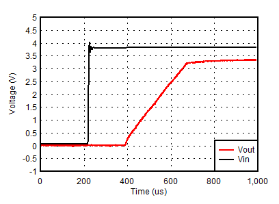
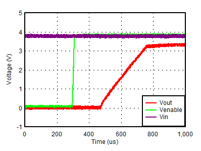
VIN = 3.8 V, VOUT = 3.3 V, IOUT = 1 mA
Figure 6-35 VIN Power-Up
GUID-FA2502D9-43BA-4260-8E7D-0967A6166DCB-low.gif
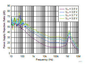
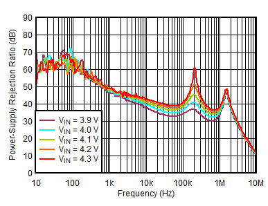
VOUT = 3.3 V, IOUT = 500 mA, COUT = 2.2 µF
Figure 6-37 PSRR vs Frequency and VIN
GUID-17FC1E1A-E22F-41EC-833E-BAC968E059EF-low.gif
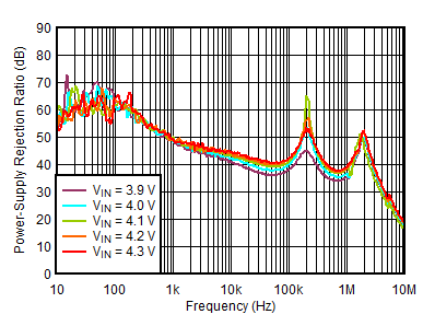
VOUT = 3.3 V, IOUT = 250 mA, COUT = 2.2 µF
Figure 6-39 PSRR vs Frequency and VIN
GUID-12A7C7E1-AFB3-47E3-AC7B-B457773AA29E-low.gif
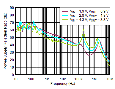
IOUT = 500 mA, COUT = 2.2 µF
Figure 6-41 PSRR vs Frequency
GUID-FCBD8027-3C41-4F2B-BACB-66FBD041F934-low.gif
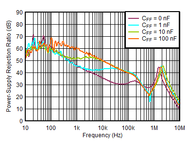
VIN = 3.8 V, VOUT = 3.3 V, IOUT = 500 mA
Figure 6-43 PSRR vs Frequency and CFF
GUID-45B7B2D3-8957-471B-8719-3E7483D0178C-low.gif
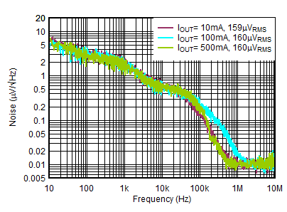
VIN = 3.8 V, VOUT = 3.3 V, COUT = 2.2 µF, VRMS BW = 10 Hz to 100 kHz
Figure 6-45 Output Spectral Noise Density vs Frequency and IOUT
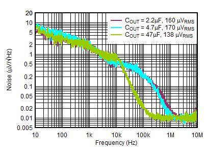
GUID-01FEF41B-8114-4279-B0F0-B1CA65ED0F20-low.gif
VIN = 3.8 V, VOUT = 3.3 V, IOUT = 100 mA, CFF = 0 µF, VRMS BW = 10 Hz to 100 kHz
Figure 6-47 Output Spectral Noise Density vs Frequency and COUT
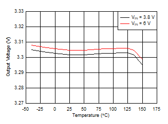
GUID-6643486B-C278-40C3-BC83-0A5688E8999D-low.gif
VOUT = 3.3 V, IOUT = 1 mA
Figure 6-2 Output Voltage vs Ambient Temperature
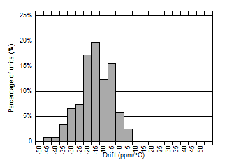
GUID-066693EB-D5D3-4DBD-AEF8-47AF3BBAA1B5-low.gif
0.65-V, 3.3-V, and 5-V options, IOUT = 1 mA
Figure 6-4 Temperature Drift Histogram (–40°C to +25°C)
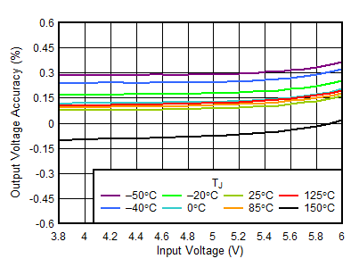
GUID-68F14633-AE73-417E-B158-E24EC44B1E53-low.gif
VOUT = 3.3 V, IOUT = 1 mA
Figure 6-6 3.3-V Line Regulation vs VIN
GUID-298FA8F9-189C-4010-82FE-51BD4E1290E3-low.gif
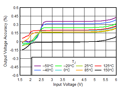
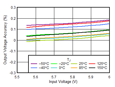
VOUT = 5.5 V, IOUT = 1 mA
Figure 6-8 5.5-V Line Regulation vs VIN
GUID-B4D9425C-9E66-480C-B16B-3BB994BC9501-low.gif
Figure 6-10 0.55-V Dropout Voltage vs IOUT
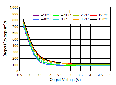
GUID-31AE8E51-A4F7-4D2D-8984-F9576A977C3C-low.gif
IOUT = 500 mA
Figure 6-12 VDO vs VOUT
GUID-5DBC97AC-B842-4472-A571-B2DF7F34E01E-low.gif
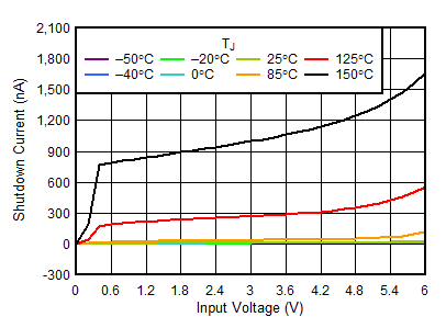
VEN = 0 V
Figure 6-14 ISHDN vs VIN
GUID-51A0B003-73E1-471F-9182-21153D7FE8D4-low.gif
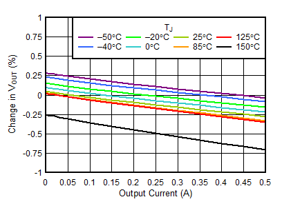
VIN = 3.8 V, VOUT = 3.3 V
Figure 6-16 3.3-V Load Regulation vs IOUT
GUID-3950ED05-F9BB-406D-B83F-948613E0E0A7-low.gif
VIN = 6 V, VOUT = 5.5 V
Figure 6-18 5.5-V Load Regulation vs IOUT
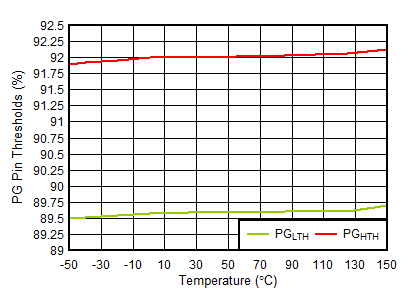
GUID-0C87177C-64DB-4079-B3AF-8DFDDD38B9D8-low.gif
 
Figure 6-20 PGLTH and PGHTH vs Temperature
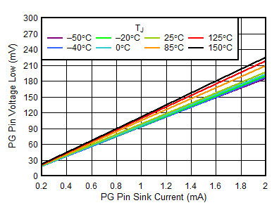
GUID-07536AE6-A14E-4FF8-B313-0539D257704A-low.gif
VIN = 3.8 V, VOUT = 3.3 V
Figure 6-22 VOL(PG) vs PG Pin Sink Current
GUID-01B02F53-978A-4FA8-A745-088F6189CD7E-low.gif
 
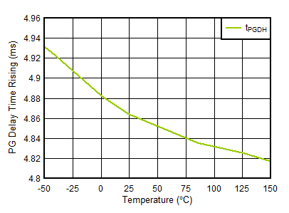
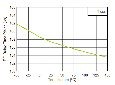
Figure 6-24 tPGDH vs Temperature
GUID-5F239EDB-698F-4831-A66F-9445D6D62AEE-low.gif
 
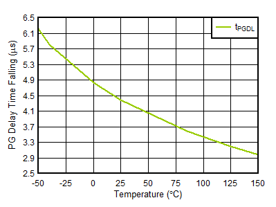
Figure 6-26 tPGDL vs Temperature
GUID-BF9E1012-6CDF-4BCC-8227-EE5E398E3A0B-low.gif
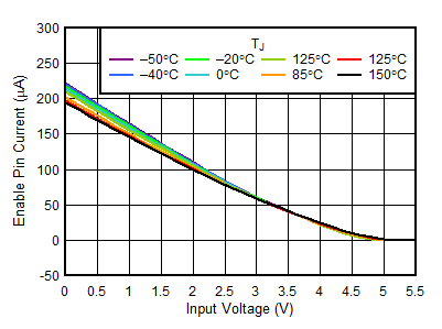
VEN = 5.5 V
Figure 6-28 IEN vs VIN
GUID-B1CDC2C2-966A-4363-A916-1ECA19638753-low.gif
VOUT = 0.55 V, IOUT = 1 mA, VIN slew rate = 1 V/µs
Figure 6-30 0.55-V Line Transient
GUID-5F67490C-A18A-42E5-9FBC-BB2152A48B55-low.gif
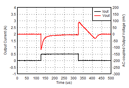
VIN = 3.8 V, VOUT = 3.3 V, IOUT slew rate = 1 A/µs
Figure 6-32 3.3-V, 1-mA to 500-mA Load Transient
GUID-8A0216C1-AE09-4A44-91F3-FB73883B3336-low.gif
VIN = 5.5 V, VOUT = 5 V, IOUT slew rate = 1 A/µs
Figure 6-34 5-V, 1-mA to 500-mA Load Transient
GUID-D09F5568-6F50-4A6F-A697-E537C8BACD46-low.gif
VIN = 3.8 V, VOUT = 3.3 V, IOUT = 1 mA
Figure 6-36 Start-Up With EN
GUID-0F8FD331-6CD2-4474-8729-7564ACED6A6D-low.gif
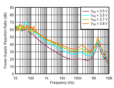
VOUT = 3.3 V, IOUT = 500 mA, COUT = 2.2 µF
Figure 6-38 PSRR vs Frequency and VIN
GUID-4125A3B3-28D7-4986-AC15-9EE7C79C0809-low.gif
VOUT = 3.3 V, IOUT = 250 mA, COUT = 2.2 µF
Figure 6-40 PSRR vs Frequency and VIN
GUID-BE5C6805-CD8E-4DC4-8DD6-FEC4D7FE3757-low.gif
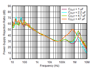
VIN = 3.8 V, VOUT = 3.3 V, IOUT = 500 mA
Figure 6-42 PSRR vs Frequency and COUT
GUID-CB87CAEE-1375-4011-A7EA-2A40F5284E97-low.gif
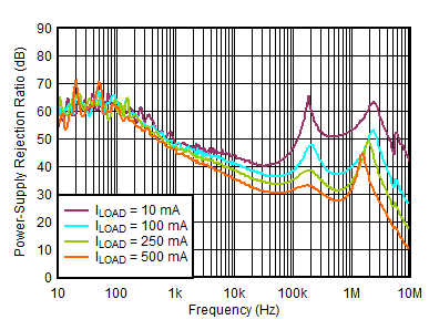
VIN = 3.8 V, VOUT = 3.3 V, COUT = 2.2 µF
Figure 6-44 PSRR vs Frequency and ILOAD
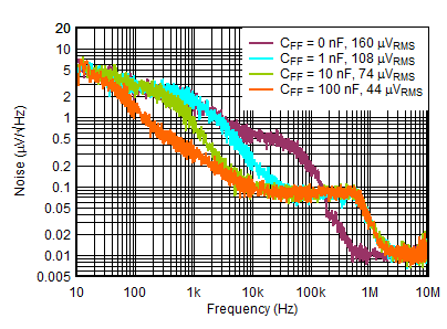
GUID-5948C06C-026A-4DDA-87F9-351B41D48804-low.gif
VIN = 3.8 V, VOUT = 3.3 V, IOUT = 500 mA, COUT = 2.2 µF, VRMS BW = 10 Hz to 100 kHz
Figure 6-46 Output Spectral Noise Density vs Frequency and CFF
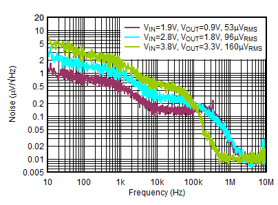
GUID-F492157F-3B4D-430F-A906-D8A6B692D9AE-low.gif
IOUT = 500 mA, COUT = 2.2 µF, VRMS BW = 10 Hz to 100 kHz
 
Figure 6-48 Output Spectral Noise Density vs Frequency