ZHCSHL0C June 2019 – May 2022 TPS745-Q1
PRODUCTION DATA
- 1 特性
- 2 应用
- 3 说明
- 4 Revision History
- 5 Pin Configuration and Functions
- 6 Specifications
- 7 Detailed Description
- 8 Application and Implementation
- 9 Power Supply Recommendations
- 10Layout
- 11Device and Documentation Support
封装选项
机械数据 (封装 | 引脚)
散热焊盘机械数据 (封装 | 引脚)
订购信息
8.2.2.1 Input Current
During normal operation, the input current to the LDO is approximately equal to the output current of the LDO. During start-up, the input current is higher as a result of the inrush current charging the output capacitor. Use Equation 6 to calculate the current through the input.
Equation 6. 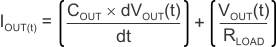
where:
- VOUT(t) is the instantaneous output voltage of the turn-on ramp
- dVOUT(t) / dt is the slope of the VOUT ramp
- RLOAD is the resistive load impedance