ZHCSEV1A February 2016 – March 2016 TPS62770
PRODUCTION DATA.
- 1 特性
- 2 应用
- 3 说明
- 4 修订历史记录
- 5 Pin Configuration and Functions
- 6 Specifications
- 7 Detailed Description
-
8 Application and Implementation
- 8.1 Application Information
- 8.2
Typical Application
- 8.2.1 System and PMOLED Supply
- 8.2.2 Step-Up Converter with 5-V Output Voltage
- 8.2.3
Step-Up Converter Operating with Constant Output Current
- 8.2.3.1 Design Requirements
- 8.2.3.2
Detailed Design Procedure
- 8.2.3.2.1 Setting The Output Voltage Of The Step-Down Converter
- 8.2.3.2.2 Programming the Output Voltage Of The Step-Up Converter
- 8.2.3.2.3 Recommended LC Output Filter
- 8.2.3.2.4 Inductor Selection Step-Down Converter
- 8.2.3.2.5 Inductor Selection Step-Up Converter
- 8.2.3.2.6 DC/DC Input and Output Capacitor Selection
- 8.2.3.3 Application Curves
- 9 Power Supply Recommendations
- 10Layout
- 11器件和文档支持
- 12机械、封装和可订购信息
8 Application and Implementation
NOTE
Information in the following applications sections is not part of the TI component specification, and TI does not warrant its accuracy or completeness. TI’s customers are responsible for determining suitability of components for their purposes. Customers should validate and test their design implementation to confirm system functionality.
8.1 Application Information
The TPS62770 is a tiny power solution for wearable applications including a 370nA ultra low Iq step-down converter, a slew rate controlled load switch and a dual mode step-up converter. The output voltage of the step-down converter can be selected between 1.0V and 3.0V. The output voltage can be changed during operation. In shutdown mode, the output of the step-down converter is pulled to GND. The integrated load switch is internally connected to the output of the step-down converter and features slew rate control during turn on phase. Once turned off, its output is connected to GND.
The dual mode step-up converter can generate a constant output voltage up to 15V, e.g. for PMOLED supply, or a constant output current, e.g. for LED back light supply. The output voltage can be adjusted up to 15V with external resistors, or set to fixed 12V by connecting the FB pin to VIN. The device features an internal over voltage protection of 17V in case the FB node is left open or tight to GND. It includes an internal rectifier and load disconnect function. When used as constant output current driver, the device offers a PWM to analog converter to scale down the reference voltage according to the duty cycle of the PWM signal.
8.2 Typical Application
8.2.1 System and PMOLED Supply
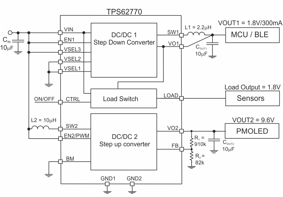 Figure 9. Step-Up Converter with Adjustable Output Voltage
spacer
spacer
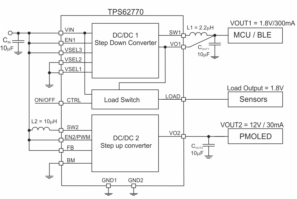 Figure 10. Step-Up Converter with Fixed 12-V Output
8.2.1.1 Design Requirements
The device is supplied by an input voltage between 2.5V and 5.5V. In wearable personal electronics this is usually a rechargeable Li-Ion battery / USB port. The step-down converter supplies the system (MCU/BLE radio). In order to supply a PMOLED display, the step-up converter must be configured to operate in constant output voltage mode with BM pin tied to GND before the step-up converter is enabled. Ideally the BM pin is hardwired to GND. The output voltage of the step-up converter is either set by an external resistor divider network (R1/R2), shown in Figure 9. The step-up converter supports an internally fixed 12V output voltage by connecting the FB pin to VIN, shown in Figure 10.
The LOAD output is internally connected to the output of the buck regulator and can supply a sensor or a sub-system, which are temporarily used. In order to achieve better supply voltage decoupling / noise reduction a capacitor can be connected on the LOAD output.
The design guideline provides a component selection to operate the device within the recommended operating conditions. Table 1 shows the components used for the application characteristic curves.
Table 1. Components for Application Characteristic Curves
| REFERENCE | DESCRIPTION | VALUE | PACKAGE CODE / SIZE [mm x mm x mm] | MANUFACTURER |
|---|---|---|---|---|
| CIN | Ceramic capacitor X5R 6.3V, GRM155R60J106ME11 | 10 µF | 0402 / 1.0 x 0.5 x 0.5 | Murata |
| COUT1 | Ceramic capacitor X5R 6.3V, GRM155R60J106ME11 | 10 µF | 0402 / 1.0 x 0.5 x 0.5 | Murata |
| COUT2 | Ceramic capacitor X5R 25V, GRM188R61E106MA73 | 10 uF | 0603 / 1.6 x 0.8 x 0.8 | Murata |
| L1 | Inductor DFE201610C | 2.2 µH | 2.0 x 1.6 x 1.0 | Toko |
| L2 | Inductor VLS302515 | 10 µH | 3.0 x 2.5 x 1.5 | TDK |
8.2.1.2 Application Curves Step-Down Converter
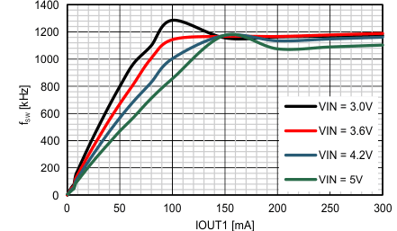
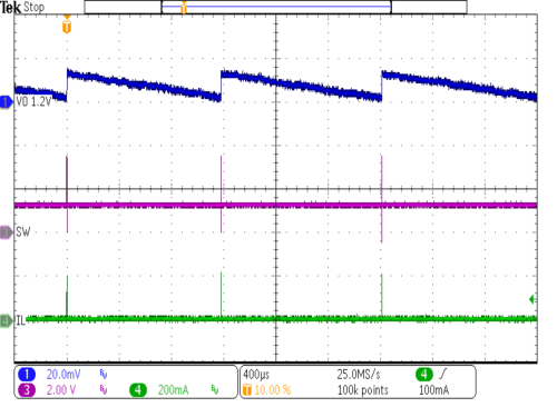
| VIN = 3.6V | IOUT = 50 µA | |
| VOUT = 1.2V | ||
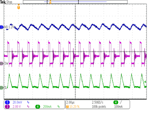
| VIN = 3.6V | IOUT = 50 mA | |
| VOUT = 1.2V | ||
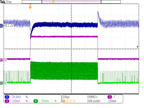
| VIN = 3.6V | IOUT = 5mA to 200mA | |
| VOUT = 1.2V | 1 µs rise/fall time | |
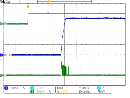
| VIN = 3.6V | IOUT = 0mA | |
| VOUT = 1.8V | ||
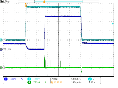
| VIN = 0 V to 3.6 V in 100 µs | EN = VIN | ||
| VOUT = 1.8V | IOUT = 0 mA | ||
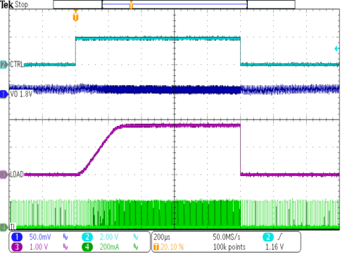
| VIN = 3.6V | IOUT1 = 5mA | ||
| VOUT = 1.8V | RLOAD = 150Ω | ||
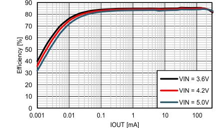
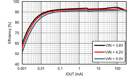
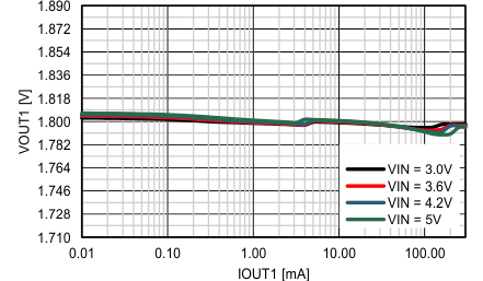
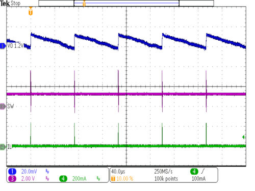
| VIN = 3.6V | IOUT = 1 mA | |
| VOUT = 1.2V | ||
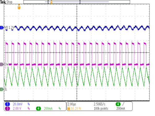
| VIN = 3.6V | IOUT = 200 mA | |
| VOUT = 1.2V | ||
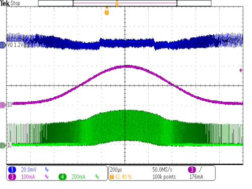
| VIN = 3.6V | IOUT = 5mA to 200mA | |
| VOUT = 1.2V | sinusodial IOUT sweep | |
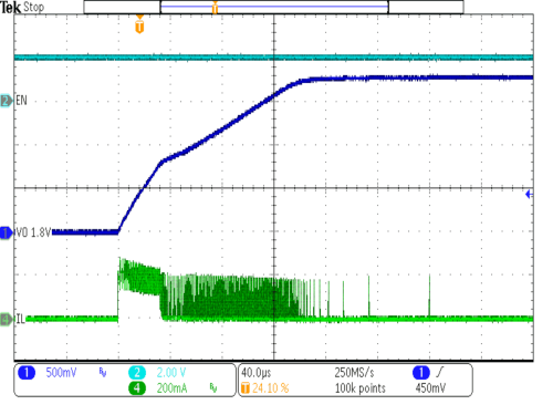
| VIN = 3.6V | IOUT = 0mA | |
| VOUT = 1.8V | EN altered from low to high | |
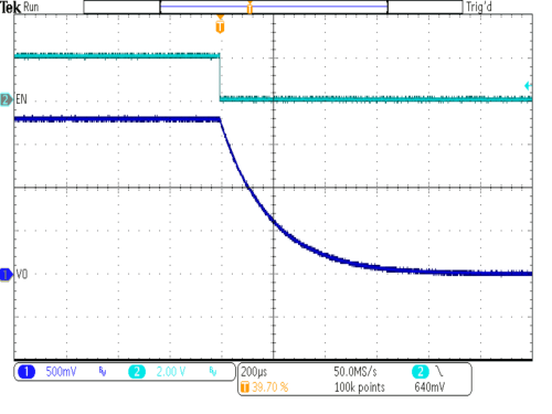
| VIN = 3.6V | IOUT = 0mA | |
| VOUT = 1.8V | ||
8.2.1.3 Application Curves Step-Up Converter Constant 12 V/15 V Output Voltage
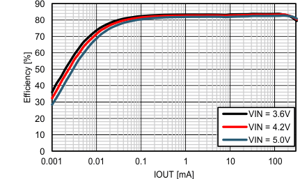
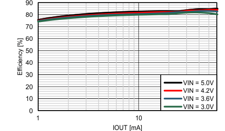 Figure 28. Efficiency vs. IOUT, VOUT = 15V
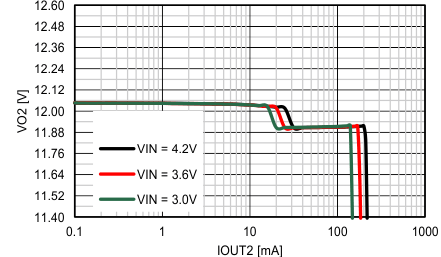
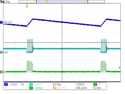
| VIN = 3.6V | IOUT2 = 2mA | |
| VOUT = 12V | L = 10µH |
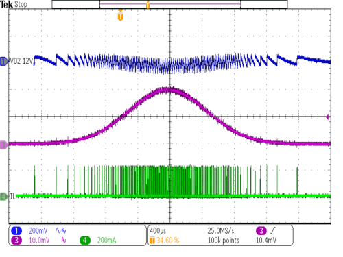
| VIN = 3.6V | IOUT2 = 0 mA to 20 mA | |
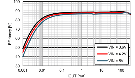
| VOUT = 12V | L = 10µH | |
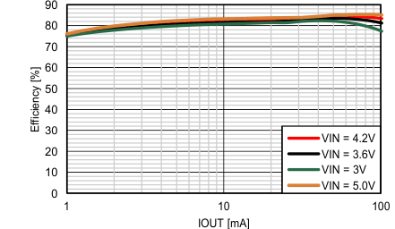 Figure 29. Efficiency vs. IOUT, VOUT = 12V
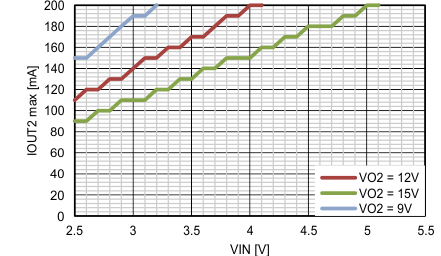
| TA = 25°C | typical switch current lmit ILIM_SW | ||
| L = 10µH | IOUT2 max @ -3% VOUT drop | ||
| COUT2 = 2x 10µF | |||
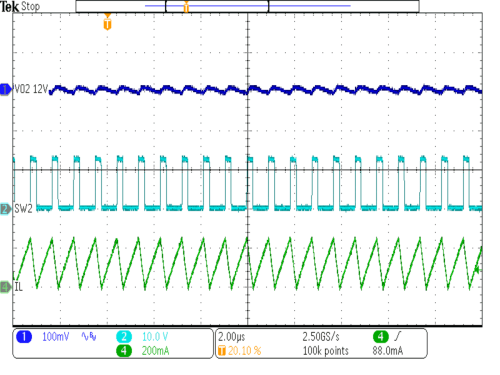
| VIN = 3.6V | IOUT2 = 30mA | |
| VOUT = 12V | L = 10µH |
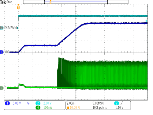
| VIN = 3.6 V | RLOAD = 1 kΩ | |
| VOUT = 12 V | L = 10 µH |
8.2.2 Step-Up Converter with 5-V Output Voltage
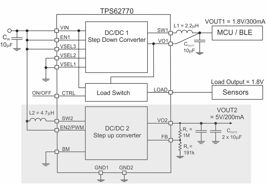 Figure 36. Step-Up Converter Providing 5-V VOUT2
8.2.2.1 Design Requirements
Table 2. Components for Application Characteristic Curves
| REFERENCE | DESCRIPTION | VALUE | PACKAGE CODE / SIZE [mm x mm x mm] | MANUFACTURER |
|---|---|---|---|---|
| CIN | Ceramic capacitor X5R 6.3V, GRM155R60J106ME11 | 10 µF | 0402 / 1.0 x 0.5 x 0.5 | Murata |
| COUT2 (2x) | Ceramic capacitor X5R 25V, GRM188R61E106MA73 | 10 uF | 0603 / 1.6 x 0.8 x 0.8 | Murata |
| L2 | Inductor VLS302515 | 4.7 µH | 3.0 x 2.5 x 1.5 | TDK |
8.2.2.2 Application Curves
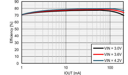
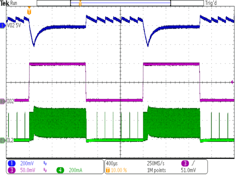
8.2.3 Step-Up Converter Operating with Constant Output Current
The step-up converter device can be configured to operate as a constant current driver e.g. to power 3 to 4 white LED's in a string. The current through the string is set by the sense resistor RSense as shown in Figure 39 To minimize the losses in the sense resistor, the device features a 200mV internal reference. This section describes an application delivering 10mA through an LED string with 4 LED's which is suitable for small display used in wearable applications.
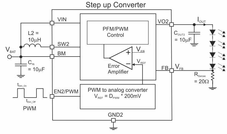 Figure 39. Step-Up Converter with Constant Output Current - Simplified Block Diagram
8.2.3.1 Design Requirements
The Sense resistor to set the maximum output current can be calculated according to Equation 3 The output current IOUT2 can be reduced by applying a PWM signal at pin EN2/PWM according to Equation 4


Where:
RSense = sense resistor in [Ω]
IOUT2 = output current in [mA]
DPWM = Dutycycle of the PWM singal at pin EN2/PWM
Table 3. Components for Application Characteristic Curves
| REFERENCE | DESCRIPTION | VALUE | PACKAGE CODE / SIZE [mm x mm x mm] | MANUFACTURER |
|---|---|---|---|---|
| CIN | Ceramic capacitor X5R 6.3V, GRM155R60J106ME11 | 10 µF | 0402 / 1.0 x 0.5 x 0.5 | Murata |
| COUT2 | Ceramic capacitor X5R 25V, GRM188R61E106MA73 | 10 uF | 0603 / 1.6 x 0.8 x 0.8 | Murata |
| L2 | Inductor VLS302515 | 10 µH | 3.0 x 2.5 x 1.5 | TDK |
| D1-D4 | LED LTW-E670DS | n/a | Lite ON |
8.2.3.2 Detailed Design Procedure
8.2.3.2.1 Setting The Output Voltage Of The Step-Down Converter
The output voltage is set with the VSEL1-3 pins according to Output Voltage Setting Step-Down Converter. No further external components are required.
8.2.3.2.2 Programming the Output Voltage Of The Step-Up Converter
There are two ways to set the output voltage of the step-up converter. When the FB pin is connected to the input voltage, the output voltage is fixed to 12 V. This function reduces the external components to minimize the solution size. The second way is to use an external resistor divider to set the desired output voltage.
By selecting the external resistor divider R1 and R2, as shown in Equation 5, the output voltage is programmed to the desired value. When the output voltage is regulated, the typical voltage at the FB pin is VREF of 795 mV.

Where:
VOUT is the desired output voltage
VREF is the internal reference voltage at the FB pin
8.2.3.2.3 Recommended LC Output Filter
Table 4. Recommended LC Output Filter Combinations for the Step-Down Converter
| INDUCTOR VALUE [µH](2) | OUTPUT CAPACITOR VALUE [µF](1) | ||
|---|---|---|---|
| 10 µF | 22 µF | ||
| 2.2 | √(3) | √ | |
8.2.3.2.4 Inductor Selection Step-Down Converter
The inductor value affects its peak-to-peak ripple current, the PWM-to-PFM transition point, the output voltage ripple and the efficiency. The selected inductor has to be rated for its DC resistance and saturation current. The inductor ripple current (ΔIL) decreases with higher inductance and increases with higher VIN or VOUT and can be estimated according to Equation 6.
Equation 7 calculates the maximum inductor current under static load conditions. The saturation current of the inductor should be rated higher than the maximum inductor current, as calculated with Equation 7. This is recommended because during a heavy load transient the inductor current rises above the calculated value. A more conservative way is to select the inductor saturation current above the high-side MOSFET switch current limit, ILIMF.


With:
f = Switching Frequency
L = Inductor Value
ΔIL= Peak to Peak inductor ripple current
ILmax = Maximum Inductor current
In DC/DC converter applications, the efficiency is essentially affected by the inductor AC resistance (i.e. quality factor) and by the inductor DCR value. Increasing the inductor value produces lower RMS currents, but degrades transient response. For a given physical inductor size, increased inductance usually results in an inductor with lower saturation current.
The total losses of the coil consist of both the losses in the DC resistance (RDC) and the following frequency-dependent components:
- The losses in the core material (magnetic hysteresis loss, especially at high switching frequencies)
- Additional losses in the conductor from the skin effect (current displacement at high frequencies)
- Magnetic field losses of the neighboring windings (proximity effect)
- Radiation losses
8.2.3.2.5 Inductor Selection Step-Up Converter
The step-up converter is optimized to work with an inductor values of 10 µH. Follow Equation 8 to Equation 10 to calculate the inductor’s peak current for the application. To calculate the current in the worst case, use the minimum input voltage, maximum output voltage, and maximum load current of the application. To have enough design margin, choose the inductor value with -30% tolerance, and a low power-conversion efficiency for the calculation.
In a step-up regulator, the inductor dc current can be calculated with Equation 8.

Where:
VOUT = output voltage
IOUT = output current
VIN = input voltage
η = power conversion efficiency, use 80% for most applications
The inductor ripple current is calculated with the Equation 9 for an asynchronous step-up converter in continuous conduction mode (CCM).

Where:
ΔIL(P-P) = inductor ripple current
L = inductor value
f SW = switching frequency
VOUT = output voltage
VIN = input voltage
Therefore, the inductor peak current is calculated with Equation 10.

The following inductor series from different suppliers have been used:
Table 6. List Of Inductors
| CONVERTER | INDUCTANCE [µH] | DIMENSIONS [mm3] | INDUCTOR TYPE | SUPPLIER(1) | |
|---|---|---|---|---|---|
| Step-down | 2.2 | 2.9 x 1.6 x 1.0 | DFE201610C | TOKO | |
| 2.2 | 2.0 × 1.25 × 1.0 | MIPSZ2012D 2R2 | FDK | ||
| 2.2 | 2.0 x 1.2 x 1.0 | MDT2012CH2R2 | TOKO | ||
| Step-up | 10 | 2.0x1.6x1.2 | VLS201610 | TDK | |
| 10 | 3.0 x 2.5 x 1.5 | VLS302515 | TDK | ||
| 4.7 | 3.0 x 2.5 x 1.5 | VLS302515 | TDK | ||
| 4.7 | 2.0 x 1.6 x 1.5 | VLS201612 | TDK | ||
8.2.3.2.6 DC/DC Input and Output Capacitor Selection
Ceramic capacitors with low ESR values have the lowest output voltage ripple and are recommended. The output capacitor requires either an X7R or X5R dielectric. Y5V and Z5U dielectric capacitors, aside from their wide variation in capacitance over temperature, become resistive at high frequencies. At light load currents, the converter operates in Power Save Mode and the output voltage ripple is dependent on the output capacitor value and the PFM peak inductor current. A 10 µF ceramic capacitor is recommended as input capacitor.
Table 7 shows a list of tested input/output capacitors.
Table 7. List Of Capacitors
| REFERENCE | DESCRIPTION | VALUE | PACKAGE CODE / SIZE [mm x mm x mm] | MANUFACTURER(1) |
|---|---|---|---|---|
| CIN | Ceramic capacitor X5R 6.3V, GRM155R60J106ME11 | 10µF | 0402 / 1.0 x 0.5 x 0.5 | Murata |
| COUT1 | Ceramic capacitor X5R 6.3V, GRM155R60J106ME11 | 10µF | 0402 / 1.0 x 0.5 x 0.5 | Murata |
| COUT2 | Ceramic capacitor X5R 25V, GRM188R61E106MA73 | 10uF | 0603 / 1.6 x 0.8 x 0.8 | Murata |
| Ceramic capacitor X5R 6.3V, GRM188R60J106ME84 | 10uF | 0603 / 1.6 x 0.8 x 0.8 | Murata |
8.2.3.3 Application Curves
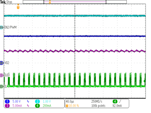
| VIN = 3.6V | RSense= 20Ω | |||
| EN2/PWM = high | 4 LEDs in series | |||
| D = 100%, ILED = 10mA | L = 10µH | |||
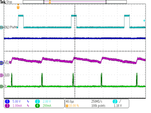
| VIN = 3.6V | RSense= 20 Ω | |
| tDim_On = 15 µs, tDim_Off = 135 µs | 4 LED's in series | |
| D = 10%, TDIim = 140 µs, ILED = 1 mA | L = 10 µH | |
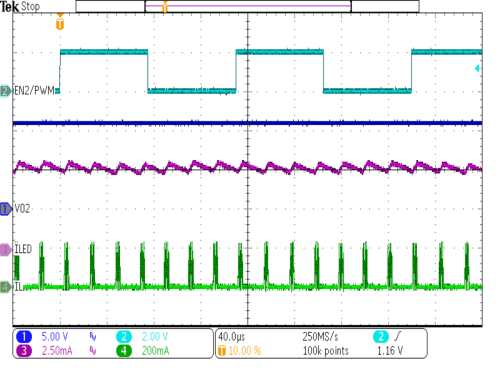
| VIN = 3.6V | RSense= 20Ω | |
| tDim_On = 75 µs, tDim_Off = 75µs | 4 LED's in series | |
| D = 50%, TDIim = 140µs, ILED = 5mA | L = 10µH | |
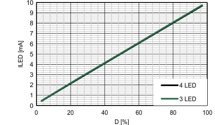
| VIN = 3.6V | RSense= 20 Ω | |
| TA = 25°C | LED's in string configuration | |
| TDIim = 50 µs (F = 20kHz) | L = 10 µH | |